Difference between revisions of "Ettus USRP E300 Embedded Family Hardware Resources"
(→China RoHS) |
(→Physical Specifications) |
||
| Line 546: | Line 546: | ||
====E313==== | ====E313==== | ||
* 186 x 280 x 106 mm | * 186 x 280 x 106 mm | ||
| + | |||
| + | ==Battery Specifications (E312 Only)== | ||
| + | Battery Specifications: [[File:E312 Battery Spec Sheet 20170426.pdf]] | ||
==Environmental Specifications== | ==Environmental Specifications== | ||
Revision as of 14:56, 27 April 2017
Contents
- 1 Device Overview
- 2 Key Features
- 3 Daughterboard Specifications
- 4 RF Specifications
- 5 Hardware Specifications
- 6 Physical Specifications
- 7 Battery Specifications (E312 Only)
- 8 Environmental Specifications
- 9 Schematics
- 10 Key Component Datasheets
- 11 Mechanical Information
- 12 FPGA
- 13 Interfaces and Connectivity
- 14 Certifications
- 15 Certificate of Volatility
- 16 SD Card Images
- 17 WiFi Network Connectivity
- 18 Additional Resources
- 19 Downloads
- 20 USRP Embedded Series FAQ
Device Overview
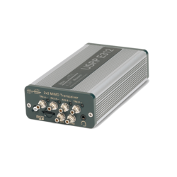
The USRP E31x offers a portable stand-alone SDR platform designed for field deployment. The flexible 2x2 MIMO AD9361 transceiver from Analog Devices provides up to 56 MHz of instantaneous bandwidth and spans frequencies from 70 MHz – 6 GHz to cover multiple bands of interest.
Key Features
E310
|
E312
|
E313
|
Daughterboard Specifications
E31x MIMO XCVR board
The USRP E31x MIMO XCVR daughterboard features an integrated MIMO capable RF frontend.
Tuning
The RF frontend has individually tunable receive and transmit chains. Both transmit and receive can be used in a MIMO configuration. For the MIMO case, both receive frontends share the RX LO, and both transmit frontends share the TX LO. Each LO is tunable between 50 MHz and 6 GHz.
Gains
All frontends have individual analog gain controls. The receive frontends have 76 dB of available gain; and the transmit frontends have 89.5 dB of available gain. Gain settings are application specific, but it is recommended that users consider using at least half of the available gain to get reasonable dynamic range.
LO lock status
The frontends provide a lo-locked sensor that can be queried through the UHD API.
// assumes 'usrp' is a valid uhd::usrp::multi_usrp::sptr instance
// get status for rx frontend
usrp->get_rx_sensor("lo-locked");
// get status for tx frontend
usrp->get_tx_sensor("lo-locked");
Filter and Antenna Switches
The transmit and receive filter banks uses switches to select between the available filters. These paths are also dependent on the antenna switch settings. Incorrectly setting the switches generally results in attenuated input / output power. Receive filters are band pass (series high & low pass filters), transmit filters are low pass.
Source code related to controlling the filter band and antenna switches resides in e300_impl.c. Specifically, refer to methods e300_impl::_update_bandsel, e300_impl::_update_atrs, e300_impl::_update_gpio, and e300_impl::_update_enables. Generally, these methods set the switches depending on the state of transmit and receive streams.
The following sections provide switch setting tables for antenna and filter selection for frontends A & B receive and transmit paths. For futher details refer to the schematics.
Side A Filter and Antenna Switches
Note: X = don't care, T = If full duplex, set bits according to transmit table, otherwise don't care. Filter range A – B will be selected if A <= freq < B.
Receive
| RX Port | RX Filter (MHz) | VCTXRX2_V1,V2 | VCRX2_V1,V2 | RX2_BANDSEL[2:0] | RX2B_BANDSEL[1:0] | RX2C_BANDSEL[1:0] |
|---|---|---|---|---|---|---|
| TRX-A | < 450 | 01 | 10 | 101 | XX | 01 |
| TRX-A | 450 – 700 | 01 | 10 | 011 | XX | 11 |
| TRX-A | 700 – 1200 | 01 | 10 | 001 | XX | 10 |
| TRX-A | 1200 – 1800 | 01 | 10 | 000 | 01 | XX |
| TRX-A | 1800 – 2350 | 01 | 10 | 010 | 11 | XX |
| TRX-A | 2350 – 2600 | 01 | 10 | 100 | 10 | XX |
| TRX-A | 2600 – 6000 | 01 | 01 | XXX | XX | XX |
| RX2-A | 70 – 450 | TT | 01 | 101 | XX | 01 |
| RX2-A | 450 – 700 | TT | 01 | 011 | XX | 11 |
| RX2-A | 700 – 1200 | TT | 01 | 001 | XX | 10 |
| RX2-A | 1200 – 1800 | TT | 01 | 000 | 01 | XX |
| RX2-A | 1800 – 2350 | TT | 01 | 010 | 11 | XX |
| RX2-A | 2350 – 2600 | TT | 01 | 100 | 10 | XX |
| RX2-A | >= 2600 | TT | 10 | XXX | XX | XX |
Transmit
| TX Port | TX Filter (MHz) | VCTXRX2_V1,V2 | TX_ENABLE2A,2B | TX_BANDSEL[2:0] |
|---|---|---|---|---|
| TRX-A | < 117.7 | 10 | 01 | 111 |
| TRX-A | 117.7 – 178.2 | 10 | 01 | 110 |
| TRX-A | 178.2 – 284.3 | 10 | 01 | 101 |
| TRX-A | 284.3 – 453.7 | 10 | 01 | 100 |
| TRX-A | 453.7 – 723.8 | 10 | 01 | 011 |
| TRX-A | 723.8 – 1154.9 | 10 | 01 | 010 |
| TRX-A | 1154.9 – 1842.6 | 10 | 01 | 001 |
| TRX-A | 1842.6 – 2940.0 | 10 | 01 | 000 |
| TRX-A | >= 2940.0 | 11 | 10 | XXX |
Note: Although the transmit filters are low pass, this table describes UHD's tuning range for selecting each filter path. The table also includes the required transmit enable state.
Side B Filter and Antenna Switches
Note: X = don't care, T = If full duplex, set bits according to transmit table, otherwise don't care. Filter range A – B will be selected if A <= freq < B.
Receive
| RX Port | RX Filter (MHz) | VCTXRX1_V1,V2 | VCRX1_V1,V2 | RX1_BANDSEL[2:0] | RX1B_BANDSEL[1:0] | RX1C_BANDSEL[1:0] |
|---|---|---|---|---|---|---|
| TRX-B | < 450 | 10 | 01 | 100 | XX | 10 |
| TRX-B | 450 – 700 | 10 | 01 | 010 | XX | 11 |
| TRX-B | 700 – 1200 | 10 | 01 | 000 | XX | 01 |
| TRX-B | 1200 – 1800 | 10 | 01 | 001 | 10 | XX |
| TRX-B | 1800 – 2350 | 10 | 01 | 011 | 11 | XX |
| TRX-B | 2350 – 2600 | 10 | 01 | 101 | 01 | XX |
| TRX-B | 2600 – 6000 | 10 | 10 | XXX | XX | XX |
| RX2-B | 70 – 450 | TT | 10 | 100 | XX | 10 |
| RX2-B | 450 – 700 | TT | 10 | 010 | XX | 11 |
| RX2-B | 700 – 1200 | TT | 10 | 000 | XX | 01 |
| RX2-B | 1200 – 1800 | TT | 10 | 001 | 10 | XX |
| RX2-B | 1800 – 2350 | TT | 10 | 011 | 11 | XX |
| RX2-B | 2350 – 2600 | TT | 10 | 101 | 01 | XX |
| RX2-B | >= 2600 | TT | 01 | XXX | XX | XX |
Transmit
| TX Port | TX Filter (MHz) | VCTXRX1_V1,V2 | TX_ENABLE1A,1B | TX1_BANDSEL[2:0] |
|---|---|---|---|---|
| TRX-B | < 117.7 | 00 | 01 | 111 |
| TRX-B | 117.7 – 178.2 | 00 | 01 | 110 |
| TRX-B | 178.2 – 284.3 | 00 | 01 | 101 |
| TRX-B | 284.3 – 453.7 | 00 | 01 | 100 |
| TRX-B | 453.7 – 723.8 | 00 | 01 | 011 |
| TRX-B | 723.8 – 1154.9 | 00 | 01 | 010 |
| TRX-B | 1154.9 – 1842.6 | 00 | 01 | 001 |
| TRX-B | 1842.6 – 2940.0 | 00 | 01 | 000 |
| TRX-B | >= 2940.0 | 11 | 10 | XXX |
Note: Although the transmit filters are low pass, the following table describes UHD's tuning range for selecting each filter path. The table also includes the required transmit enable states.
RF Specifications
RF Performance
- SSB/LO Suppression -35/50 dBc
- Phase Noise 3.5 GHz 1.0 deg RMS
- Phase Noise 6 GHz 1.5 deg RMS
- Power Output >10dBm
- IIP3 (@ typ NF) -20dBm
- Typical Noise Figure <8dB
Hardware Specifications
- Ettus Research recommends to always use the latest stable version of UHD
E310
- Current Hardware Revision: 1
- Minimum version of UHD required: 3.8.0
- Required version on the host computer must match what is running on the E310
E312
- Current Hardware Revision: 1
- Minimum version of UHD required: 3.8.5
- Required version on the host computer must match what is running on the E312
E313
- Current Hardware Revision: 1
- Minimum version of UHD required: 3.8.0
- Required version on the host computer must match what is running on the E313
Physical Specifications
Dimensions
E310
- 133 x 68 x 26.4 mm
E312
- 133 x 68.2 x 31.8 mm
E313
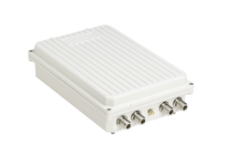
- 186 x 280 x 106 mm
Battery Specifications (E312 Only)
Battery Specifications: File:E312 Battery Spec Sheet 20170426.pdf
Environmental Specifications
Operating Temperature Range
- E310 0-40 °C
- E312 0-40 °C
- E313 -40-71 °C
Operating Humidity Range
- 10% to 90% non-condensing
Schematics
E310
Key Component Datasheets
| Part Number | Description | Schematic ID (Page) |
|---|---|---|
| Motherboard | ||
| TXS02612RTWR | SDIO PORT EXPANDER | U23 (2) |
| XC7Z020-1CLG484CES9919 | FPGA | U11 (2,3,4,8,11,13) |
| Xilinx Zynq Product Page | FPGA | - |
| USB3340-EZK-TR | ULPI Transceiver | U33 (5) |
| AK4571VQP | Audio CODEC | U30 (6) |
| FT230XQ-R | UART Interface | U32 (6) |
| 88E1512 | Gigabit Ethernet Transceiver | U13 (7) |
| 24LC024/SN | EEPROM | U5 (9) |
| DS1339,SM | Real-Time Clock | U6 (9) |
| ADT7408 | Temperature Sensor | U8 (9) |
| MPU-9150 | Motion Processing Unit | U3 (9) |
| InvenSense MPU-9150 Product Page | Motion Processing Unit | U3 (9) |
| BMP180 | Digital pressure sensor | U4 (9) |
| BQ24192 | Adapter Charger | U1 (10) |
| TPS54478 | Step-Down Switcher | U20 (10) |
| MAX6510HAUT-T | Temperature Switches | U35 (10) |
| ATTINY88-MU | Microcontroller | U18 (10) |
| TPS61253YFF | Step-Up Converter | U19 (10) |
| AMY-6M | GPS Module | U12 (6) |
| Daughterboard | ||
| Part Number | Description | Schematic ID (Page) |
| AD9361 Product Page | 2 x 2 RF Agile Transceiver | U8 (3) |
| 24AA256 | EEPROM | U15 (2) |
| TC-1-43A+ | RF Transformer | T6 (3); T5 (3); T4 (3) |
| TC1-1-13M+ | RF Transformer | T7 (3); T10 (3); T1 (3) |
| TPS62140 | Step-Down Converter | U19 (4) |
| ADP1753ACPZ-R7 | Linear Regulator | U17 (4); U18 (4) |
| SGA-4563Z | MMIC AMPLIFIER | U12 (5); U4 (5) |
| SKY13418-485LF | Antenna Switch | U13 (5); U3 (5); U16 (5); U2 (5); U10 (6); U5 (6) |
| SKY13373-460LF | SP3T Switch | U11 (6); U9 (6); U6 (6); U7 (6); SW4 (7); SW1 (7) |
| MGA-81563 | Amplifier | U14 (5); U1 (5) |
| LFCN-5850+ | Low Pass Filter | FL32 (5); FL1 (5) |
| LFCN-2750+ | Low Pass Filter | FL37 (5); FL4 (5) |
| LFCN-2250+ | Low Pass Filter | FL23 (6); FL20 (6) |
| LFCN-1700+ | Low Pass Filter | FL40 (5); FL2 (5) |
| LFCN-1575+ | Low Pass Filter | FL25 (6); FL17 (6) |
| LFCN-1000+ | Low Pass Filter | FL33 (5); FL9 (5); FL27 (6); FL15 (6) |
| LFCN-575+ | Low Pass Filter | FL36 (5); FL5 (5) |
| LFCN-530+ | Low Pass Filter | FL29 (6); FL13 (6) |
| LFCN-400+ | Low Pass Filter | FL38 (5); FL3 (5); FL30 (6); FL11 (6) |
| LFCN-225 | Low Pass Filter | FL39 (5); FL6 (5) |
| LFCN-160+ | Low Pass Filter | FL34 (5); FL8 (5) |
| LFCN-80+ | Low Pass Filter | FL35 (5); FL7 (5) |
| HFCN-1600+ | High Pass Filter | FL22 (6); FL19 (6) |
| HFCN-1100+ | High Pass Filter | FL24 (6); FL16 (6) |
| HFCN-650+ | High Pass Filter | FL26 (6); FL14 (6) |
| HFCN-440+ | High Pass Filter | FL28 (6); FL12 (6) |
| BFCN-2435+ | Bandpass Filter | FL21 (6); FL18 (6) |
| FDG6301N | Dual N-Channel, Digital FET | Q8 (7); Q5 (7) |
| HSMS-8202 | Mixer Diodes | CR1 (7); CR2 (7); CR3 (7); CR4 (7) |
| LP5900TL | Linear Regulator | U25 (8) |
| ADP150AUJZ-3.0 | Linear Regulator | U22 (8) |
| AD5662RBJ | 16-Bit nanoDAC | U21 (8) |
| SN74AUP1T57 | Voltage Translator | U27 (8); U28 (8); U29 (8) |
Request a detailed whitepaper covering features and components from [email protected]
Mechanical Information
Weight
E310
- 375 g
E312
- 446 g
E313
- 1.8 kg
Drawings
E310
- File:E310 Dimensional Sketches.pdf
- File:cu e310 motherboard cca.pdf
- File:cu E310 daughtercard cca.pdf
- File:cu usrp-e310.pdf
E312
E313
- File:USRP E313 Dimension Pole Mount.pdf
- File:USRP E313 Dimension Surface Mount.pdf
- File:USRP E313 Mounting Accessory Assembly Guide.pdf
- Media:USRP E313 USB conduit interface.png
FPGA
- Utilization statistics are subject to change between UHD releases. This information is current as of UHD 3.9.4 and was taken directly from Xilinx Vivado 2014.4.
E310/E312/E313
1. Slice Logic
--------------

+----------------------------+-------+-----------+-------+
|          Site Type         |  Used | Available | Util% |
+----------------------------+-------+-----------+-------+
| Slice LUTs                 | 36203 |     53200 | 68.05 |
|   LUT as Logic             | 28108 |     53200 | 52.83 |
|   LUT as Memory            |  8095 |     17400 | 46.52 |
|     LUT as Distributed RAM |   870 |           |       |
|     LUT as Shift Register  |  7225 |           |       |
| Slice Registers            | 36562 |    106400 | 34.36 |
|   Register as Flip Flop    | 36562 |    106400 | 34.36 |
|   Register as Latch        |     0 |    106400 |  0.00 |
| F7 Muxes                   |   376 |     26600 |  1.41 |
| F8 Muxes                   |   125 |     13300 |  0.93 |
+----------------------------+-------+-----------+-------+

3. Memory
---------

+-------------------+------+-----------+-------+
|     Site Type     | Used | Available | Util% |
+-------------------+------+-----------+-------+
| Block RAM Tile    |   97 |       140 | 69.28 |
|   RAMB36/FIFO*    |   90 |       140 | 64.28 |
|     RAMB36E1 only |   90 |           |       |
|   RAMB18          |   14 |       280 |  5.00 |
|     RAMB18E1 only |   14 |           |       |
+-------------------+------+-----------+-------+
* Note: Each Block RAM Tile only has one FIFO logic available and therefore can accommodate only one FIFO36E1 or one FIFO18E1. However, if a FIFO18E1 occupies a Block RAM Tile, that tile can still accommodate a RAMB18E1


4. DSP
------

+----------------+------+-----------+-------+
|    Site Type   | Used | Available | Util% |
+----------------+------+-----------+-------+
| DSPs           |  120 |       220 | 54.54 |
|   DSP48E1 only |  120 |           |       |
+----------------+------+-----------+-------+
Interfaces and Connectivity
- 10/100/1000 BASE-T Ethernet
- Stereo audio out, mono mic in
- Integrated GPS receiver
- Host USB support
- 9-axis IMU
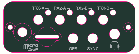
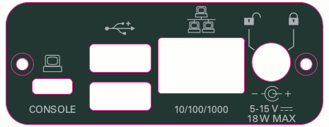
Front Panel
Rear Panel
|
|
GPIO
|
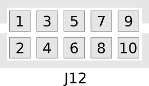
Pin Mapping
|
|
Power on state
The hardware power on state and UHD initial state for the front-panel GPIOs is high-Z. For the E3xx, there are no external pull-ups/pull-downs for the GPIO pins, but the FPGAs do have them and they are configured as follows: E3xx: pull-down.
- Please see the E3x0/X3x0 GPIO API for information on configuring and using the GPIO bus.
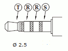
Audio
Certifications
RoHS
As of December 1st, 2010 all Ettus Research products are RoHS compliant unless otherwise noted. More information can be found at http://ettus.com/legal/rohs-information
China RoHS
Management Methods for Controlling Pollution Caused by Electronic Information Products Regulation
Chinese Customers
National Instruments is in compliance with the Chinese policy on the Restriction of Hazardous Substances (RoHS) used in Electronic Information Products. For more information about the National Instruments China RoHS compliance, visit ni.com/environment/rohs_china.
Certificate of Volatility
E310
E312
SD Card Images
This folder linked above contains SD card images and the SDK (OE cross-compiler build environment) for the USRP E31x. There is a manifest file that shows which packages, and which versions, are included in the OE build within each folder.
The "alpha", "beta", "e3xx-release-001", "e310-release-002", "e3xx-release-3" folders contain older versions which are currently obsolete. We do not suggest that customers use these files. These versions are no longer supported. They are provided here for archival purposes only.
The current version is Release 4, which located in the "e3xx-release-4" folder. We recommend the customers use this version. It is fine if you are already successfully using an older version, but at some point it is recommended that you upgrade to this current version so that you benefit from the latest bug fixes, new features, stability improvements, and other enhancements.
The Release 4 image includes UHD 3.9.2 and GNU Radio 3.7.9, and also includes the corresponding FPGA image file.
Note: An 8 GB SD card is required for the Release 4 image.
The SD card image contains both the FPGA image and the OS for the E31x. The FPGA images are located in the file system of the E31x in the /usr/local/share/uhd/images folder.
There are two SD card image files for each version of the image, which include the text "-dev" and "-demo" in the filename. The "-dev" flavor lacks some graphical packages, such as X Windows and QT, which the "-demo" flavor includes. The two flavors are otherwise functionally equivalent, although the "-demo" flavor takes some additional space on the SD card and some additional memory to run.
The Release 4 image comes in two varieties. The variety that you will need depends on the product number of your E31x, which is printed on the bottom of the device.
For the E310, the product number will be 156333X-01L, where X is a letter from A to Z. For devices where X is A, B, C, D, the images under the "ettus-e3xx-sg1" folder should be used. For devices where X is E or later, the images under the "ettus-e3xx-sg3" folder should be used. You must use the appropriate image for your specific device. The incorrect image will not work, and will only boot as far as the U-Boot boot loader before stopping.
For the E312, the product number will be 140605X-01L, where X is a letter from A to Z. The images under the "ettus-e3xx-sg3" folder should be used for all E312 devices.
You can burn the image to an SD card using either the "dd" or the "bmaptool" tool. Instructions on how to use these tools are at the links below.
The SD image files have an *.xz extension, as they are compressed using the LZMA/LZMA2 compression algorithms. You can uncompress these files with tools such as 7-Zip and the XZ Utils. Please see the links below for further information.
7-Zip
XZ Utils
The folder structure is listed below.
.
|-- alpha
|   |-- dizzy-test
|   |   |-- oecore-x86_64-armv7ahf-vfp-neon-toolchain-nodistro.0.manifest
|   |   |-- oecore-x86_64-armv7ahf-vfp-neon-toolchain-nodistro.0.sh
|   |   |-- sdimage-gnuradio-demo.direct.xz
|   |   `-- sdimage-gnuradio-dev.direct.xz
|   |-- fido-rfnoc-test
|   |   |-- oecore-x86_64-armv7ahf-vfp-neon-toolchain-nodistro.0.manifest
|   |   |-- oecore-x86_64-armv7ahf-vfp-neon-toolchain-nodistro.0.sh
|   |   |-- sdimage-gnuradio-demo.direct.xz
|   |   |-- sdimage-gnuradio-demo.direct.xz.md5
|   |   |-- sdimage-gnuradio-dev.direct.xz
|   |   `-- sdimage-gnuradio-dev.direct.xz.md5
|   |-- fido-test
|   |   |-- ettus-e3xx-sg1
|   |   |   |-- sdimage-gnuradio-demo.direct.xz
|   |   |   |-- sdimage-gnuradio-demo.direct.xz.md5
|   |   |   |-- sdimage-gnuradio-dev.direct.xz
|   |   |   `-- sdimage-gnuradio-dev.direct.xz.md5
|   |   |-- ettus-e3xx-sg3
|   |   |   |-- sdimage-gnuradio-demo.direct.xz
|   |   |   |-- sdimage-gnuradio-demo.direct.xz.md5
|   |   |   |-- sdimage-gnuradio-dev.direct.xz
|   |   |   `-- sdimage-gnuradio-dev.direct.xz.md5
|   |   |-- oecore-x86_64-armv7ahf-vfp-neon-toolchain-nodistro.0.manifest
|   |   `-- oecore-x86_64-armv7ahf-vfp-neon-toolchain-nodistro.0.sh
|   `-- fosphor-testing
|       |-- fosphor.direct.xz
|       |-- oecore-x86_64-armv7ahf-vfp-neon-toolchain-nodistro.0.host.manifest
|       |-- oecore-x86_64-armv7ahf-vfp-neon-toolchain-nodistro.0.sh
|       |-- oecore-x86_64-armv7ahf-vfp-neon-toolchain-nodistro.0.target.manifest
|       |-- sdimage-gnuradio-demo.direct.xz
|       |-- sdimage-gnuradio-demo.direct.xz.md5
|       |-- sdimage-gnuradio-dev.direct.xz
|       `-- sdimage-gnuradio-dev.direct.xz.md5
|-- beta
|   |-- dizzy-test
|   |   |-- oecore-x86_64-armv7ahf-vfp-neon-toolchain-nodistro.0.manifest
|   |   |-- oecore-x86_64-armv7ahf-vfp-neon-toolchain-nodistro.0.sh
|   |   |-- sdimage-gnuradio-demo.direct.xz
|   |   `-- sdimage-gnuradio-dev.direct.xz
|   `-- dizzy-test-wifi
|       `-- sdimage-gnuradio-dev.direct.xz
|-- e310-release-002
|   |-- oecore-x86_64-armv7ahf-vfp-neon-toolchain-nodistro.0.manifest
|   |-- oecore-x86_64-armv7ahf-vfp-neon-toolchain-nodistro.0.sh
|   |-- sdimage-gnuradio-demo.direct.xz
|   |-- sdimage-gnuradio-demo.direct.xz.md5sum
|   |-- sdimage-gnuradio-dev.direct.xz
|   `-- sdimage-gnuradio-dev.direct.xz.md5sum
|-- e3xx-release-001
|   |-- e300-gnuradio-dev-image-release1.bz
|   `-- nodistro-eglibc-x86_64-gnuradio-dev-image-armv7ahf-vfp-neon-toolchain-nodistro.0.sh
|-- e3xx-release-3
|   |-- oecore-x86_64-armv7ahf-vfp-neon-toolchain-nodistro.0.manifest
|   |-- oecore-x86_64-armv7ahf-vfp-neon-toolchain-nodistro.0.sh
|   |-- sdimage-gnuradio-demo.direct.xz
|   `-- sdimage-gnuradio-dev.direct.xz
`-- e3xx-release-4
    |-- ettus-e3xx-sg1
    |   |-- sdimage-gnuradio-demo.direct.xz
    |   |-- sdimage-gnuradio-demo.direct.xz.md5
    |   |-- sdimage-gnuradio-dev.direct.xz
    |   `-- sdimage-gnuradio-dev.direct.xz.md5
    |-- ettus-e3xx-sg3
    |   |-- sdimage-gnuradio-demo.direct.xz
    |   |-- sdimage-gnuradio-demo.direct.xz.md5
    |   |-- sdimage-gnuradio-dev.direct.xz
    |   `-- sdimage-gnuradio-dev.direct.xz.md5
    |-- oecore-x86_64-armv7ahf-vfp-neon-toolchain-nodistro.0.manifest
    `-- oecore-x86_64-armv7ahf-vfp-neon-toolchain-nodistro.0.sh
WiFi Network Connectivity
Below are instructions on setting up a USB WiFi adapter with the E3xx. We have tested the "Edimax EW-7811Un", however many USB based WiFi adapters should be supported.
First verify the USB WiFI adapter is found by running lsusb.
Example output from lsusb for the "Edimax EW-7811Un" WiFi adapter:
Bus 001 Device 003: ID 7392:7811 Edimax Technology Co., Ltd EW-7811Un 802.11n Wireless Adapter [Realtek RTL8188CUS]
If the USB adapter is found, proceed with installation and configuration procedure:
1. Run the command below. Enter the passphrase and hit <Enter>.
wpa_passphrase <SSID> >> /etc/wpa_supplicant.conf`
2. In the file /etc/wpa_supplicant.conf, edit the entry created above to look like the text below (just add what is missing).
network={
       ssid="YOUR_SSID"
       psk=HASH_VALUE
       key_mgmt=WPA-PSK
       proto=RSN WPA
       pairwise=CCMP TKIP
       group=CCMP TKIP
}
3. Run the command:
wpa_supplicant -B -D nl80211 -i wlan0 -c /etc/wpa_supplicant.conf
4. Run the command:
udhcpc -i wlan0
Additional Resources
Application Notes
Third-party Resources
Downloads
USRP Embedded Series FAQ
General USRP E31x Questions
Q: What data rate is supported for continuous sample streaming to a desktop or laptop host-PC? A: Unlike host-based SDRs such as the USRP B, N, and X Series devices, the USRP E Series devices are not intended for continuous streaming of high bandwidth data to a desktop or laptop host-PC. The SDR application runs on an embedded CPU with limited processing capability. Users should leverage the FPGA using tools such as RFNoC to offload compute intensive algorithms that process high bandwidth samples.
Q: What data rate is supported between FPGA to the ARM processor? A: Due to the limited performance of the embedded processor, the maximum data rate from the FPGA to ARM cores is approximately 10 MS/s, and will vary with the processing load on the CPU. The AD9631 RFIC is capable of capturing 56 MHz of bandwidth. Processing signals at full bandwidth requires implementing algorithms on the FPGA.
Q: What is the purpose of the 1 GbE port? A: The E Series can run a DHCP client on the 1 GigE interface to enable connection to a larger network for remote access by another computer. Power over Ethernet is also supported on the E313.
USRP E313 Questions
Q: Which environmental tests were performed? A: The USRP E313 is tested against multiple environmental standards to ensure operation in outdoor conditions. These test include ingress protection, temperature, humidity, mechanical shock, random vibration, and altitude. Detailed specifications are provided in the [link data sheet].
Q: How do I protect external devices connected to the host USB port?
|
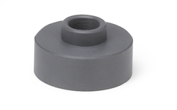
A: A circular conduit interface is provided in the kit. This component has large and small threaded ends. The small end connects to the USB port on the USRP E313. The user will need to connect their own waterproof structure to the large end to protect the USB device. Since requirements for external devices vary greatly, the conduit interface serves as a flexible starting point for users to build their own solution. See the Media:USRP E313 Dimension Pole Mount.pdf of the conduit interface for details. |
Q: How do I protect unused ports? A: All ports come with protective end caps that should be left in place on unused ports.
Q: Why is a DC power supply not included? A: The RJ45 port supports Power over Ethernet and is intended as the primary power supply option. However, users can still use a DC power supply. Since requirements for supplying DC power in outdoor scenarios can vary greatly, a waterproof sleeve for the DC port is provided as a starting point for users to design their own solution. A waterproof sleeve for the RJ45 port is also provided.
Q: Do the RF inputs have lightning protection? A: The DC and PoE power inputs have surge and lightning protection, but the N-type RX/TX inputs and SMA GPS input do not. Users should design antenna lightning protection based on their application requirements.


