Difference between revisions of "N200/N210"
(→Datasheets) |
(→Key Component Datasheets) |
||
| Line 88: | Line 88: | ||
!Part Number | !Part Number | ||
!Description | !Description | ||
| − | !Schematic ID | + | !Schematic ID (Page) |
| − | + | ||
|- | |- | ||
|[http://www.analog.com/media/en/technical-documentation/data-sheets/AD9777.pdf AD9777] | |[http://www.analog.com/media/en/technical-documentation/data-sheets/AD9777.pdf AD9777] | ||
|Dual Channel, 16-Bit DAC | |Dual Channel, 16-Bit DAC | ||
| − | | | + | |U3 (1) |
| − | + | ||
|- | |- | ||
|[http://www.ti.com/lit/ds/symlink/ads62p45.pdf ADS62P4X] | |[http://www.ti.com/lit/ds/symlink/ads62p45.pdf ADS62P4X] | ||
|Dual Channel, 14-Bit ADC | |Dual Channel, 14-Bit ADC | ||
| − | | | + | |U2 (1) |
| − | + | ||
|- | |- | ||
|[http://www.xilinx.com/support/documentation/data_sheets/ds529.pdf XC3SD3400AFG676] | |[http://www.xilinx.com/support/documentation/data_sheets/ds529.pdf XC3SD3400AFG676] | ||
|FPGA | |FPGA | ||
| − | | | + | |U1 (2,8,9,10,11,12) |
| − | + | ||
|- | |- | ||
|AD56x3 | |AD56x3 | ||
| | | | ||
| − | | | + | |U4, U5 (3) |
| − | + | ||
|- | |- | ||
|[http://www.analog.com/media/en/technical-documentation/data-sheets/AD9510.pdf AD9510] | |[http://www.analog.com/media/en/technical-documentation/data-sheets/AD9510.pdf AD9510] | ||
|Clock Distribution IC | |Clock Distribution IC | ||
| − | | | + | |U9 (4) |
| − | + | ||
|- | |- | ||
|[http://download.siliconexpert.com/pdfs/2008/04/26/isys/lsi/ds06-161gphy_et1011c_09-28-2007.pdf ET1011C2] | |[http://download.siliconexpert.com/pdfs/2008/04/26/isys/lsi/ds06-161gphy_et1011c_09-28-2007.pdf ET1011C2] | ||
|Gigabit Ethernet Transceiver | |Gigabit Ethernet Transceiver | ||
| − | | | + | |U12 (6) |
| − | + | ||
|- | |- | ||
|[http://www.cypress.com/file/43236/download CY7C1354C] | |[http://www.cypress.com/file/43236/download CY7C1354C] | ||
|Pipelined SRAM | |Pipelined SRAM | ||
| − | | | + | |U19 (7) |
| − | + | ||
|- | |- | ||
|[http://www.ti.com/lit/ds/symlink/max232.pdf MAX232] | |[http://www.ti.com/lit/ds/symlink/max232.pdf MAX232] | ||
|Drivers/Receiver | |Drivers/Receiver | ||
| − | | | + | |U25 (10) |
| − | + | ||
|- | |- | ||
|} | |} | ||
Revision as of 14:41, 14 May 2016
Contents
- 1 Device Overview
- 2 Key Features
- 3 Compatible Daughterboards
- 4 RF Specifications
- 5 Hardware Specifications
- 6 Clocks and Samples Rates
- 7 Physical Specifications
- 8 Environmental Specifications
- 9 Schematics
- 10 Key Component Datasheets
- 11 Mechanical Info
- 12 FPGA
- 13 Interfaces and Connectivity
- 14 Multiple Device Configuration
- 15 Certifications
- 16 Certificate of Volatility
- 17 Downloads (FPGA images, E310 images, etc.)
- 18 Application Notes
Device Overview
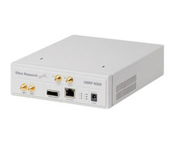
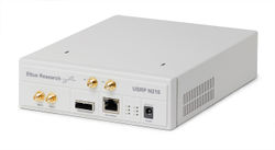
The USRP Network Series offers high-bandwidth, high-dynamic range processing capability. The Gigabit Ethernet interface of the USRP Network Series allows high-speed streaming capability up to 50 MS/s in both directions (8-bit samples). These features, combined with plug-and-play MIMO capability make the USRP Network an ideal candidate for software defined radio systems with demanding performance requirements.
Key Features
N200
|
N210
|
Compatible Daughterboards
- SBX-40
- UBX-40
- WBX-40
- CBX-40
- LFRX / LFTX
- BasicRX / BasicTX
- TVRX2
- DBSRX2
RF Specifications
RF Performance (with WBX)
- SSB/LO Suppression -35/50 dBc
- Phase Noise 1.8 GHz 10kHz -80 dBc/Hz
- Phase Noise 1.8 GHz 100kHz -100 dBc/Hz
- Phase Noise 1.8 GHz 1MHz -137 dBc/Hz
- Power Output 15 dBm
- IIP3 (@ typ NF) 0 dBm
- Typical Noise Figure 5 dB
Hardware Specifications
N200
- Details
N210
- Details
Clocks and Samples Rates
- FIXME NEEL
Physical Specifications
Dimensions
22 x 16 x 5 cm
Environmental Specifications
Operating Temperature Range
- N200/N210 0-40 °C
Schematics
N200/N210
Key Component Datasheets
| Part Number | Description | Schematic ID (Page) |
|---|---|---|
| AD9777 | Dual Channel, 16-Bit DAC | U3 (1) |
| ADS62P4X | Dual Channel, 14-Bit ADC | U2 (1) |
| XC3SD3400AFG676 | FPGA | U1 (2,8,9,10,11,12) |
| AD56x3 | U4, U5 (3) | |
| AD9510 | Clock Distribution IC | U9 (4) |
| ET1011C2 | Gigabit Ethernet Transceiver | U12 (6) |
| CY7C1354C | Pipelined SRAM | U19 (7) |
| MAX232 | Drivers/Receiver | U25 (10) |
Mechanical Info
Weight
1.2 kg
Drawings
FPGA
- Utilization statistics are subject to change between UHD releases, current as of UHD 3.9.4
N200
Device utilization summary:
---------------------------

Selected Device : 3sd1800afg676-5

 Number of Slices:                    18356  out of  16640   110% (*)
 Number of Slice Flip Flops:          20466  out of  33280    61%
 Number of 4 input LUTs:              32968  out of  33280    99%
    Number used as logic:             28511
    Number used as Shift registers:    3945
    Number used as RAMs:                512
 Number of IOs:                         338
 Number of bonded IOBs:                 331  out of    519    63%
    IOB Flip Flops:                     342
 Number of BRAMs:                        41  out of     84    48%
 Number of GCLKs:                         6  out of     24    25%
 Number of DCMs:                          1  out of      8    12%
 Number of DSP48s:                       31  out of     84    36%
N210
Device utilization summary:
---------------------------

Selected Device : 3sd3400afg676-5

 Number of Slices:                    18349  out of  23872    76%
 Number of Slice Flip Flops:          20475  out of  47744    42%
 Number of 4 input LUTs:              32986  out of  47744    69%
    Number used as logic:             28529
    Number used as Shift registers:    3945
    Number used as RAMs:                512
 Number of IOs:                         338
 Number of bonded IOBs:                 331  out of    469    70%
    IOB Flip Flops:                     342
 Number of BRAMs:                        41  out of    126    32%
 Number of GCLKs:                         6  out of     24    25%
 Number of DCMs:                          1  out of      8    12%
 Number of DSP48s:                       31  out of    126    24%
Interfaces and Connectivity
N200/N210
- Gigabit Ethernet
Multiple Device Configuration
- [ADD]
Certifications
RoHS
As of December 1st, 2010 all Ettus Research products are RoHS compliant unless otherwise noted. More information can be found at http://ettus.com/legal/rohs-information
Certificate of Volatility
N200/N210
Downloads (FPGA images, E310 images, etc.)


