N300/N310
Contents
- 1 Notice
- 2 Device Overview
- 3 Key Features
- 4 RF Specifications
- 5 Power
- 6 Hardware Specifications
- 7 Physical Specifications
- 8 Environmental Specifications
- 9 Schematics
- 10 Mechanical Drawings
- 11 GPSDO
- 12 FPGA
- 13 Interfaces and Connectivity
- 14 Certifications
- 15 Certificate of Volatility
- 16 Downloads
- 17 Choosing a Host Interface
- 18 International Power Supply Options
- 19 Guidance on SFP+ Adapters for Fiber Connectivity on USRP N310
Notice
When you receive a brand-new device, it is strongly recommended that you download the most recent filesystem image from the Ettus Research website and write it to the SD card that comes with the unit. It is not recommended that you use the SD card from the factory as-is. Instructions on downloading the latest filesystem image and writing it to the SD card are listed below.
Device Overview
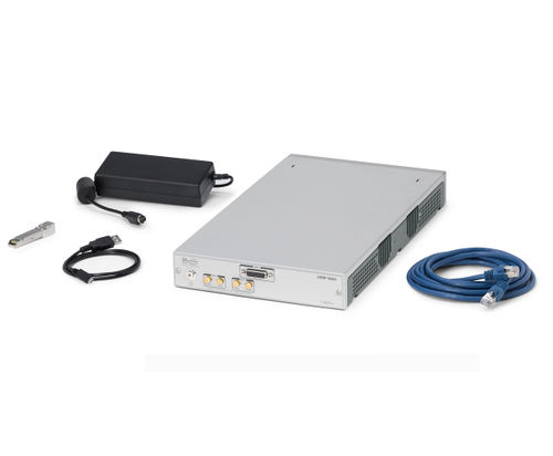
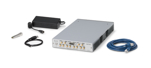
The USRP N310 is a networked software defined radio that provides reliability and fault-tolerance for deployment in large scale and distributed wireless systems. This device simplifies control and management of a network of radios by introducing the unique capability to remotely perform tasks such as debugging, updating software, rebooting, factory resetting, self-testing, and monitoring system health. The USRP N310 is an all-in-one device that includes two AD9371 transceivers, the Zynq-7100 SoC baseband processor, two SFP+ ports, a built-in GPSDO module, and various other peripheral and synchronization features.
Key Features
N300
|
|
N310
|
|
RF Specifications
Transmitter
- Number of channels: 4
- Frequency Range: 10 MHz to 6 GHz
- Maximum instantaneous bandwidth: 100 MHz
- Minimum frequency step
- 7.32 Hz @ 122.88 MHz sample rate
- 7.45 Hz @ 125 MHz sample rate
- 9.15 Hz @ 153.6 MHz sample rate
- Maximum output power (P out ): See Table 1
- Gain range
- -30 dB to 25 dB (10 MHz to 300 MHz)
- -30 dB to 20 dB (300 MHz to 6 GHz)
- Gain step: 1 dB
- Supported I/Q sample rates:
- 122.88 MHz, 125 MHz, 153.6 MHz
- Spurious-free dynamic range (SFDR) > 50 dBc
- Output third-order intercept (OIP3) See Table 2
| Frequency | Maximum Output Power |
|---|---|
| 10 MHz to 500 MHz | +16 dBm |
| 500 MHz to 1 GHz | +18 dBm |
| 1 GHz to 4 GHz | +18 dBm |
| 4 GHz to 6 GHz | +12 dBm |
Table 1: Maximum Output Power
| Frequency | Output Third-Order Intercept (IP3) |
|---|---|
| 10 MHz to 2 GHz | > 30 dBm |
| 2 GHz to 4 GHz | > 20 dBm |
| 4 GHz to 6 GHz | > 10 dBm |
Table 2: Third-Order Intercept (IP3)
Receiver
- Number of channels: 4
- Frequency Range: 10 MHz to 6 GHz
- Maximum instantaneous bandwidth: 100 MHz
- Minimum frequency step
- 7.32 Hz @ 122.88 MHz sample rate
- 7.45 Hz @ 125 MHz sample rate
- 9.15 Hz @ 153.6 MHz sample rate
- Gain step: 1
- Maximum recommended input power (P in ) 1 dB: -15 dBm
- Noise figure: See Table 3
- Spurious-free dynamic range (SFDR): > 50 dBc
- Third-order intermodulation distortion (IMD3) See Table 4
- Supported I/Q sample rates
- 122.88 MHz, 125 MHz, 153.6 MHz
| Frequency | TX/RX Noise Figure | RX2 Noise Figure |
|---|---|---|
| 1.8 GHz | 6.8 dB | 5.8 dB |
| 2.4 GHz | 7.5 dB | 6.5 dB |
| 4.4 GHz | 7.0 dB | 5.5 dB |
| 5.8 GHz | 6.4 dB | 6.4 dB |
Table 3: Noise Figure
| Frequency | RX IMD3 |
|---|---|
| 0.5 GHz to 3 GHz | < -80 dBc |
| 3 GHz to 4 GHz | < -74 dBc |
| 4 GHz to 6 GHz | < -81 dBc |
Table 4: RX Third-Order Intermodulation Distortion (IMD3)
- Noise figure is measured at maximum gain state on receiver signal path.
Onboard DRAM
- DDR3 Memory size
- 2,048 MB (PL)
- 1,024 MB (PS)
Power
You must use either the Level VI Efficiency power supply provided in the shipping kit, or another UL listed ITE power supply marked LPS, with the USRP N310.
- Input voltage: 12 VDC
- Input current: 7.0 A, maximum
- Typical power consumption: 50 W to 80 W, varies by application
Hardware Specifications
- Ettus Research recommends to always use the latest stable version of UHD
- If you need to clean the module, wipe it with a dry towel.
N310
- Current Hardware Revision: A
- Minimum version of UHD required: 3.11.0.0
- Due to product compliance restrictions on products with TPM (Trusted Platform Module) components to a few countries, the USRP N310 is available in two variants:
- Standard variant with TPM (P/N 785067-01)
- Non-TPM variant (P/N 786465-01)
Clocking and Sampling Rates
There are three master clock rates (MCR) supported on the N310: 122.88 MHz; 125.0 MHz; 153.6 MHz.
The sampling rate must be an integer decimation rate of the MCR. Ideally, this decimation factor should be an even number. An odd decimation factor will result in additional unwanted attenuation (roll-off from the CIC filter in the DUC and DDC blocks in the FPGA). The valid decimation rates are between 1 and 1024.
For the MCR of 122.88 MHz, the achievable sampling rates using an even decimation factor are 122.88, 61.44, 30.72, 20.48, 15.36, 12.288, 10.24, 8.777, 7.68 Msps, ... 120.0 Ksps.
For the MCR of 125.0 MHz, the achievable sampling rates using an even decimation factor are 125.0, 62.5, 31.25, 20.833, 15.625, 12.5, 10.41666, 8.9286 Msps, ... 122.07 Ksps.
For the MCR of 153.6 MHz, the achievable sampling rates using an even decimation factor are 156.3, 78.15, 39.075, 26.05, 19.5375, 15.63, 13.025, 11.16429 Msps, ... 152.637 Ksps
If the desired sampling rate is not directly supported by the hardware, then it will be necessary to re-sample in software. This can be done in C++ using libraries such as Liquid DSP [1], or can be done in GNU Radio, in which there are three blocks that perform sampling rate conversion.
Physical Specifications
Dimensions
(L × W × H)
- 35.71 cm × 21.11 cm × 4.37 cm
- 14.06 in. × 8.31 in. × 1.72 in.
Weight
- 3.13 kg
Environmental Specifications
Operating Temperature Range
- N310: 0 to 50 °C
Storage Temperature Range
- N310: -40 to 70 °C
Operating Humidity Range
- 10% to 90% non-condensing
Schematics
N300/N310
- Motherboard: File:USRP N310 N300 MB Schematic.pdf
- Daughterboard: File:USRP N310 N300 DB Schematic.pdf
Mechanical Drawings
N300
N310
GPSDO
- Support GPSDO NMEA Strings
Sensors
You can query the lock status with the gps_locked sensor, as well as obtain raw NMEA sentences using the gps_gprmc, and gps_gpgga sensors. Location information can be parsed out of the gps_gpgga sensor by using gpsd or another NMEA parser.
Specifications
| Module Specifications | |
|---|---|
| 1 PPS Timing Accuracy from GPS receiver | <8ns to UTC RMS (1-Sigma) GPS Locked |
| Holdover Stability (1 week with GPS) | <±50us over 3 Hour Period @+25°C (No Motion, No Airflow) |
| 1 PPS Output | 3.3VDC CMOS |
| Serial Port | TTL Level, GPS NMEA Output with 1Hz or 5Hz update rate, Integrated into UHD |
| GPS Frequency | L1, C/A 1574MHz |
| GPS Antenna | Active (3V compatible) or Passive (0dB to +30dB gain) |
| GPS Receiver | 65 Channels, QZSS, SBAS WAAS, EGNOS, MSAS capable
Supports Position and Hold over-determined clock mode |
| Sensitivity | Acquisition -148dBm, Tracking -165dBm |
| TTFF | Cold Start: <32 sec, Warm Start: 1 sec, Hot Start: 1 sec |
| ADEV | 10s: <7E-011
10Ks: <2E-012 (GPS Locked, 25°C, no motion, no airflow) |
| Warm Up Time / Stabilization Time | <10 min at +25C to 1E-09 Accuracy |
| Supply Voltage (Vdd) | 3.3V Single-Supply, +0.2V/-0.15V |
| Power Consumption | <0.16W |
| Operating Temperature | -10°C to +70°C |
| Storage Temperature | -45C to 85C |
| Oscillator Specifications (internal) | |||
|---|---|---|---|
| Frequency Output of low Phase Noise crystal | 20MHz CMOS 3Vpp | ||
| 20MHz Retrace | ±2E-08 After 1 Hour @ +25°C without GPS | ||
| RF Output Amplitude | 3Vpp CMOS | ||
| 20MHz Phase Jitter (100Hz to 10MHz) | <0.135ps rms | ||
| Frequency Stability Over Temperature (0°C to +60°C) | ±0.1ppm (internal TCXO without GPS) | ||
| Warm Up Time | < 1 min at +25C | ||
| Phase Noise at 20MHz | 1Hz | -65 dBc/Hz | |
| 10Hz | -97 dBc/Hz | ||
| 100Hz | -116 dBc/Hz | ||
| 1kHz | -136 dBc/Hz | ||
| 10kHz | <-148 dBc/Hz | ||
| 100 kHz | <-155 dBc/Hz | ||
Datasheet
- Spec Sheet: http://www.jackson-labs.com/assets/uploads/main/LTE-Lite_specsheet_20MHz.pdf
- User Manual: http://www.jackson-labs.com/assets/uploads/main/LTE-Lite.pdf
FPGA
FPGA User Modifications
The Verilog code for the FPGA in the USRP N300/N310 is open-source, and users are free to modify and customize it for their needs. However, certain modifications may result in either bricking the device, or even in physical damage to the unit. Specifically, changing the I/O interface of the FPGA in any way, or modifying the pin and timing constraint files, could result in physical damage to other components on the motherboard, external to the FPGA, and doing this will void the warranty. Also, even if the PCIe interface is not being used, you cannot remove or reassign these pins in the constraint file. The constraint files should not be modified. Please note that modifications to the FPGA are made at the risk of the user, and may not be covered by the warranty of the device.
Interfaces and Connectivity
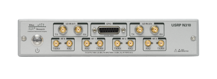
Front Panel
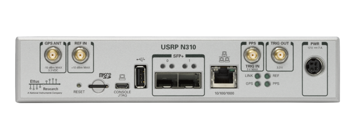
Rear Panel
Ref Clock - 10 MHz
Using an external 10 MHz reference clock, a square wave will offer the best phase noise performance, but a sinusoid is acceptable. The power level of the reference clock cannot exceed +10 dBm.
PPS - Pulse Per Second
Using a PPS signal for timestamp synchronization requires a square wave signal with the following a 5Vpp amplitude.
To test the PPS input, you can use the following tool from the UHD examples:
-
<args>are device address arguments (optional if only one USRP device is on your machine)
cd <install-path>/lib/uhd/examples ./test_pps_input –args=<args>
Front Panel GPIO
|
The GPIO port is not meant to drive big loads. You should not try to source more than 5mA per pin. The +3.3V is for ESD clamping purposes only and not designed to deliver high currents. |
Power on state
The hardware power on state and UHD initial state for the front-panel GPIOs is high-Z. For the N310, there are no external pull-ups/pull-downs for the GPIO pins, but the FPGAs do have them and they are configured as follows: N310: pull-down.
Pin Mapping
- Pin 1: +3.3V
- Pin 2: Data[0]
- Pin 3: Data[1]
- Pin 4: Data[2]
- Pin 5: Data[3]
- Pin 6: Data[4]
- Pin 7: Data[5]
- Pin 8: Data[6]
- Pin 9: Data[7]
- Pin 10: Data[8]
- Pin 11: Data[9]
- Pin 12: Data[10]
- Pin 13: Data[11]
- Pin 14: 0V
- Pin 15: 0V
Note: Please see the E3x0/X3x0/N3x0 GPIO API for information on configuring and using the GPIO bus.
Certifications
RoHS
As of December 1st, 2010 all Ettus Research products are RoHS compliant unless otherwise noted. More information can be found at http://ettus.com/legal/rohs-information
China RoHS
Management Methods for Controlling Pollution Caused by Electronic Information Products Regulation
Chinese Customers
National Instruments is in compliance with the Chinese policy on the Restriction of Hazardous Substances (RoHS) used in Electronic Information Products. For more information about the National Instruments China RoHS compliance, visit ni.com/environment/rohs_china.
Certificate of Volatility
N300/N310
Downloads
Choosing a Host Interface
10 Gigabit Ethernet
Recommended 10 Gigabit Ethernet Cards
- Intel X520-DA2 - Previous generation PCIe Gen 2 adapter. Mature and stable 10GbE adapter, works out-of-the-box with Ubuntu 14.04 LTS and 16.04 LTS
- Intel X520-DA1 - Previous generation PCIe Gen 2 adapter Mature and stable 10GbE adapter, works out-of-the-box with Ubuntu 14.04 LTS and 16.04 LTS
- Intel X710-DA2 - New PCIe Gen 3 adapter
- Intel X710-DA4 - New PCIe Gen 3 adapter
Additional Links and Resources for Intel 10GbE adapters
International Power Supply Options
The power supply provided with the USRP N310 kit is packaged with a power cord that is compatible with power outlets in the US/Japan. If you are not using the USRP N310 in the US/Japan, we recommend purchasing the International USRP N310 Power Cord set.
Guidance on SFP+ Adapters for Fiber Connectivity on USRP N310
Ettus Research currently offers direct-connect, copper cabling accessories for the USRP N310. However, it is also possible to use multi-mode fiber instead of copper connections for these devices. In this section, we will provide general guidance on the types of fiber adapters and cables that can be used with these products. General Guidance on SFP+ Adapters
The USRP N310 USRP is compatible with most brands of SFP+ fiber adapters. In some cases, other equipment in the systems such as 1/10 Gigabith Ethernet switches are only compatible with specific brands of SFP+ adapters and cables. As a general rule, we recommend checking compatibility with the switches and network cards in your system before purchasing an adapter.
Ettus Research does test the USRP N310 USRP devices with our 10 Gigabit Ethernet Connectivity Kit and a Blade Networks G8124 1/10 GigE switch. Here are is a list of known-good cables and adapters.
Ettus Research has only tested multi-mode fiber accessories.


