Debugging FPGA images
Contents
Application Note Number
AN-121
Revision History
| Date | Author | Details |
|---|---|---|
| 2016-11-28 | Nicolas Cuervo Sugandha Gupta |
Initial creation |
Abstract
This application note covers the basics to get you through the process of probing the signals inside an FPGA. In order to accomplish that, we will review briefly the 'Xilinx ChipScope Analyzer' and will apply it to one of our core RFNoC blocks: the RFNoC Signal generator. The contents of this AN could suit most of your needs while setting your debug bitstream for a RFNoC design. However, keep in mind that the topics described here are strictly related to Xilinx framework. For further information please refer to Xilinx documentation [1][2].
Overview
When you are developing your own application, you might come to the point on which you would like to build an FPGA image for your USRP. You might want to modify part of the cores, add some custom functionality, or even add your custom RFNoC block! For that you might follow tutorials such as the Building the FPGA image section of one our "getting started" guides.
But how about debugging your HDL code? This comes really handy when you want to follow closely the behavior of your signals within your hardware design. This Application Note will follow the basic steps needed to create a "chipscope image", which allow you to use the Vivado GUI visual tools to debug your design.
Before we start, this App note assumes that you have been working already with some FPGA code and you want to debug it. Being this the case, we assume that you have UHD installed, the FPGA repository cloned, the right version of Xilinx Vivado installed (by the moment this is being written we use Vivado 2015.4) and its environment initialized. If not, we assume you are familiar on how to do the previously noted procedures.
For illustration purposes, here we are going to check the status of some of the output signals of one of the RFNoC blocks we currently provide. However, the same procedure can be used to check the status of any signal within your hardware code, being input, output, or intermediate signal, and being the code a core description, a module for your library or your custom RFNoC block.
Note: Keep in mind that this procedure intends to probe the signals in a fully designed block, which has been also built into a FPGA .bit file and is running in a supported device. This is *not* intended to be a way to test directly your designed code, as building an FPGA image may take several minutes (even hours). For small functionality checks, we strongly recommend you to write a testbench for your code, which will allow you to have more iterations without the need of building and synthesizing your hardware description. You can follow the - Writing Testbenches section of our reference manual to have insights on how to write your own testbench. In addition, there is plenty of online resources (such as [8]) that provide enough information to get you started with your simulation.
Prerequisites
- Vivado (version 2015.4): As stated in the overview, you'll be working directly with HDL code that you need to build and synthesize. Depending on your target device, you may even need a non-free license (which is the case for the X3XX devices). In the case of Ettus' embedded devices, you can proceed with your design using the Vivado Webpack.
- UHD, GNURadio and gr-ettus: At the end of the debugging process we will be running the application on a physical device, and for that we need the core code downloaded and installed. UHD will serve as our device driver, GNURadio the frame on which our app will run, and gr-ettus is needed for our signal generator block. If you need guidance on this, please refer to the Creating a development environment section of our Getting started guide. If you are debugging your own RFNoC OOT module, this will have to be installed as well.
- RFNoC supported device: The whole point of chipscoping is having the ability of probing signals from a hardware design at runtime. Hence, a device where the application is going to run is needed. In this tutorial we will be using an X310 device.
Choosing your signals
At this point we assume that you have a verilog code that has been properly tested by the means of simulation/testbench, but that you want to inspect into its functionality deeper by probing its signals while it is running on a device. This could be helpful for many reasons, such as getting a deeper understanding on the state of your signal during a given transaction, which could give you an insight on how it is working (or even, can give you a lead on why it isn't!)
For this AN, we will use out block RFNoC: Signal Generator as our Unit Under Test (UUT). However, all procedures to be done can be easily transfered to your own design. In addition, as most of our block and FPGA code is written in Verilog, we will use it also in this document. So let's get started.
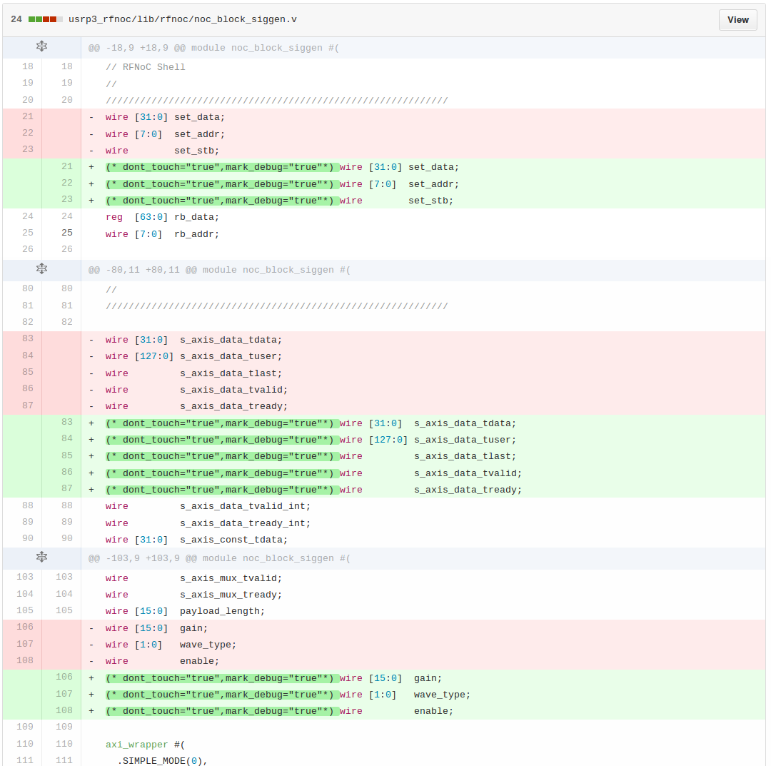
The Signal generator's code can be found under {fpga-repository}/usrp3/lib/rfnoc/. In some of our latest code releases (such as 3.10.0.0), this code is found under {fpga-repository}/usrp3_rfnoc/lib/rfnoc/. In this directory you can find the RFNoC related code that is used in the RFNoC framework. Consequently, all the HDL for the NoC blocks the we provide is located here. Now, open the file noc_block_siggen.v in your IDE or text editor of preference and give it a quick look.
As you can see, the code is not too extensive and is the comments divide it properly based on functionality. If your design is RFNoCModtool-generated, you'll get a similar preliminary structure in the verilog files for your block. For information on how to use RFNoCModtool please refer to RFNoC Development - Getting Started Guide. Normally for rather simple designs you won't have to deal with the RFNoC Shell or the AXI Wrapper configuration. However, for illustration purposes, we are going to take some of the signals from this part of the code and probe them in our debugging process. A total of 11 signals will be selected, each from a different internal stage.
Lets take a look at how this boundaries look like in the FPGA Internals. Each full RFNoC design can include several different blocks, which are also called "computation engines". The picture on the right [3] portraits the computation engine internals in a quite self explanatory fashion, although a slightly more detailed explanation about each of the internals from a Computation Engine can be found at the RFNoC Software Page:

From NoC Shell: At the top of the figure you can see the AXI Crossbar, were all the computation engines are wired up together. This is not part of our UUT in particular. However, the connection between the crossbar and our UUT - NoC Shell can be tested within our code. From here we are taking the set_data/addr/stb, which are readback registers and provide information from this interface.
- set_data
- set_addr
- set_stb
From the AXI Wrapper: our next stage from where we are taking signals is the AXI Wrapper. This can be understood as a translating stage in which the data that goes from and to the user's design is correctly encapsulated into a CHDR packet [5]. By probing this signals we expect to find out that the data that is being transported is correct, and that the transaction also takes places at the right moment.
- s_axis_data_tdata
- s_axis_data_tuser
- s_axis_data_tlast
- s_axis_data_tvalid
- s_axis_data_tready
From the signal generator design: Last but not least, we are probing signals from the UUT IP, which means that we are checking directly the value that certain lines inside the FPGA have the correct value at a certain time. In this case, we'll be checking if the wave type is according with the one selected from the host, that the gain value is propagated correctly and, clearly, if the block is generating signals when it is enable and when it isn't.
- gain
- wave_type
- enable
Setting up the code for ChipScoping
To let know Vivado that we want to probe signals, we have to go directly into the code and mark this signals for debugging. This can be done by using reserved words that describe the synthesizing attributes for a given signal. There is a variety of different attributes that you can give to any signal of your design [2], but here we are going to discuss the ones that serve most of the debugging needs:
- KEEP: This attribute prevents the signal to be optimized or absorbed into logic blocks, which would mean that the signal, even though it would be operational after synthesis, may not be accessible for probing. An example of the syntax for this attribute is as follows:
 VERILOG:
   (* keep = "true" *) wire signal_name;
   assign signal_name = in1 & in2;
 VHDL:
   signal signal_name : std_logic;
   attribute keep : string;
   attribute keep of signal_name : signal is "true";
   signal_name <= in1 and in2;
- KEEP_HIERARCHY: As well as KEEP, this attribute prevents the optimization. However, this attribute can be applied to a module or instance. By using this attribute, the synthesis tools keep the boundary on this signal static. Example:
 VERILOG
   On Module:
   (* keep_hierarchy = "yes" *) module example (in1, in2, out1, out2);
   On Instance:
   (* keep_hierarchy = "yes" *) example e0 (.in1(in1), .in2(in2), .out1(out1));
 VHDL
   On Module:
   attribute keep_hierarchy : string;
   attribute keep_hierarchy of example : architecture is "yes";
   On Instance:
   attribute keep_hierarchy : string;
   attribute keep_hierarchy of e0 : label is "yes";
- DONT_TOUCH: this attribute works just as KEEP and KEEP_HIERARCHY, with the difference that this one is forward-annotated to place and route to prevent logic optimization. In case where other attributes get into conflict with DONT_TOUCH, DONT_TOUCH takes precedence and will be applied. It also can take values yes/no and true/false. Example:
 VERILOG WIRE
   (* dont_touch = "yes" *) wire signal1;
   assign signal1 = in1 & in2;
 VERILOG MODULE
   (* DONT_TOUCH = "yes" *)
   module example (clk, in1, in2, out1);
 VHDL EXAMPLE
   signal sig1 : std_logic;
   attribute dont_touch : string;
   attribute dont_touch of sig1 : signal is "true"
- MARK_DEBUG: This is arguably the most important attribute for our current use case, because it is the one that tells Vivado which nets are going to be debugged. This also prevents optimization over the signal, and in addition prepares it to be probed during operation. Virtually this attribute could be applied to any net within the design, but there are some nets with specific properties could have protection against visibility, and can not be probed. The values for MARK_DEBUG are TRUE/FALSE. Example:
 VERILOG
   (* MARK_DEBUG = "TRUE" *) wire debug_wire;
 VHDL
   attribute MARK_DEBUG : string;
   attribute MARK_DEBUG of signal_name : signal is "TRUE";
For other attributes and options, please refer to Xilinx's documentation [1][2]. We are going to use the given almost in every case, if not always. Now, the syntax is rather simple and so is the applications to the attributes to the code. The resulting file should look as the picture on the right. When you have modified the code, you are ready to build your debug bitstream.
Building the debug bitstream
Save the project and finish Synthesis
For this test in particular you are going to need to have a DDC (Digital down converter) in addition to the UUT for visualization purposes on a host. To add this blocks into the bitstream, go to {fpga-repository}/[usrp3|usrp3_rfnoc/tools/scripts/ and inside that directory run the following command:
$ ./uhd_image_builder.py siggen ddc -g
This will set up your Vivado environment and start the build of an FPGA image with the signal generator and the DDC blocks. The option '-g' is telling the script that at some point during the build process the Vivado User Interface should be opened, as it is where we are going to set up our debug image. For uhd_image_builder.py usage and options please refer to the Wiring up computation engines and building the FPGA image section of our getting started guide, or simply run uhd_image_builder.py --help in your terminal
Note: The FPGA image building process may take over an hour.
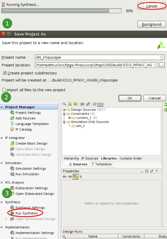
The Vivado GUI is going to come up at some point of the synthesis. Right after the Vivado GUI has opened, you can go ahead and cancel the process that is running, which is usually the last part of the synthesis (when it shows 90% done is a safe moment to cancel. See "Saving the project" figure). This is because we first have to set up the parameters for debugging and the synthesis has to be re-run. After canceling, save the project and give it a name of your choice; we are giving here the name AN_chipscope, but you can name the project whatever you like. Right after saving the project, click on 'Run Synthesis', which can be found on the left panel under Project Manager->Synthesis->Run Synthesis.
Note: Most of the time Vivado will auto-detect your highest hierarchy module, but it may happen that it just slips to it and then it will ask you which it. If this happens, you can select the verilog file according to the target device that you are chipscoping as the top module (e.g. x300.v or e300.v)
Now wait until the synthesis is finished. This won't take long, and after it finishes a window will prompted saying that the synthesis is done, and asking if you want to run the implementation. Click on cancel, as we need to setup the debugging parameters first.
Setup debug
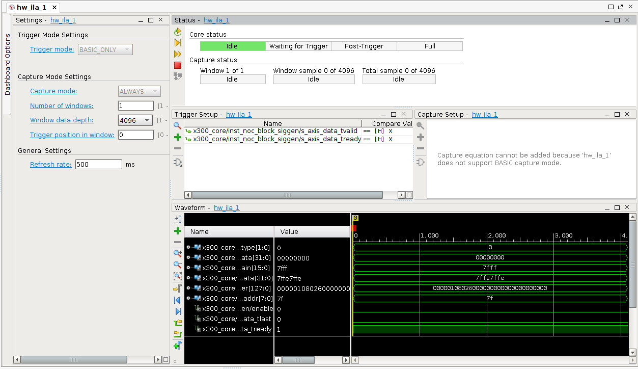
Go to Project Manager -> Synthesis -> Open Synthesized Design -> Set Up debug, and the wizard will start. Click on next until you see a window listing the nets to debug. Here, two scenarios are expected. See the figure below:
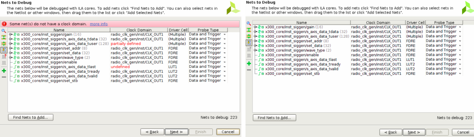
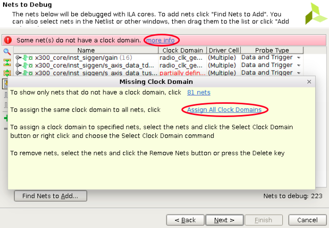
Sometimes Vivado will pick up the clock domain automatically (which is the case depicted on the right side), but there are occasions where the nets to debug aren't clearly defined under a clock domain and this cases require a little bit more of work, depending on your knowledge of your design. In this case, we know that the nets are under the same clock domain as the other signals, but in case of doubt, you'll have to go and find it out through the code. The case on the left can be solved easily by clicking on 'more info', which is just at the end of the red warning. Right after clickling, further, clearly, information will appear. In the prompted dialog, let us click on 'Assign All Clock Domains'
A window will appear where you can choose the common clock domain on which you want to have the signals. Here, in our case, we select radio_clk_gen/inst/CLK_OUT1, and that would be sufficient to continue. Accept and click next.
Right after, we have to choose the Integrated Logic Analizer - ILA Core Options [6][7]. Here we will only focus on "Sample of data depth" and "Input pipe stages"
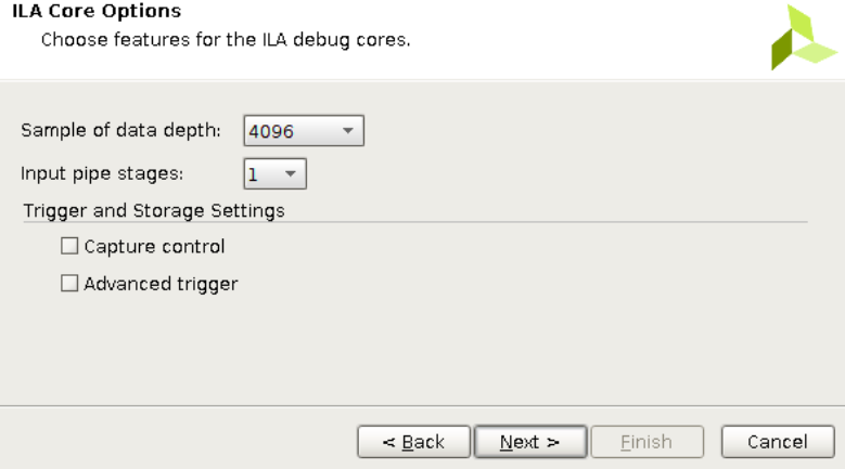
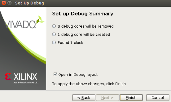
The "Sample of data depth" is the maximum number of data sample words that the ILA core can store at run time for each of the probe lines. The input pipe stages is the number of flops or registers that are added to each probe line. This basically determines how big the debug setup will be, and the amount of data that is going to be analyzed per run. Here we select 4096 for the data depth and 1 input pipe line. For further information about the ILA and its configuration, please refer to the ILA documentation [6][7]. With this, the set up is done, and you can proceed to click "next" and then "finish" to complete the wizard operation.
After the setup is finished, go to the left panel and click Project Manager->Program and Debug->Generate Bitstream. This will ask you if you want to run the implementation first, to what we answer 'Yes'. This will prepare the bitstream with which we are going to program our device and debug our design.
Running the debug bitstream in the target device
After the bitstream generation is completed successfully, it is time for us to move on and put our design into the device. On the left pannel, right below we generated our bitstream, is the "Hardware Manager". At this point, we have our X310 connected via JTAG for programming purposes, and via Ethernet (1G in this specific use case) for later usage. Now, click on 'Open Target'. If you have only one device connected, the option "auto-connect" should work just fine. Otherwise, select your device by clicking on "Open new target" and following the options in order to find the device you want. After doing so, two options should appear at the top of your Vivado window:
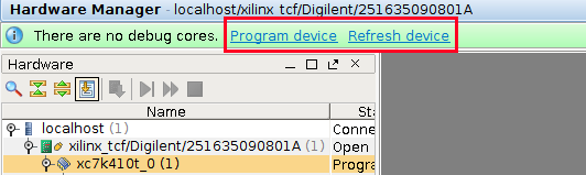
As a first step, click on "Program device". Usually, again, Vivado picks up the bitstream that you just generated. However, if you have been running multiple bitstream builds and/or have multiple Vivado projects, it is possible that you would have to look for the right bitstream. It should be under the project that you have been working during the generation of your debug bitstream.
After programing, you have to run an initialization routine on your device. A way to do this is to run a usrp probe, which will also tell us several interesting information. In a terminal, run:
$ uhd_usrp_probe
This will tell you information about the device. In our case, the last portion of the output should look like this:
   |   |    /
   |   |   |       RFNoC blocks on this device:
   |   |   |
   |   |   |   * DmaFIFO_0
   |   |   |   * Radio_0
   |   |   |   * Radio_1
   |   |   |   * SigGen_0
   |   |   |   * DUC_0
   |   |   |   * DDC_0
which tells us that the blocks Signal Generator, DUC and DDC were correctly added into the device. Keep in mind that the DmA FIFO and two instances of the radio are added by default into an X310 device. Now, go back to the Vivado GUI and click on "Refresh device" right on the top of the Vivado Window. After that, your debugging signals should appear and you are ready to start chipscoping.
Selecting Triggers
While probing your design, you probably want to know the state of a given signal right at the moment at which it or other signal changed. In some cases you can have a short simulation and you can eye-ball your signals and see if the results are as expected. However, sometimes signals change very fast or have a really short duration, making a qualitative procedure a little bit more complicated. For that case, you can set up triggers, which means that the chipscope tool will start capturing when a desired signal changes. We are going to use this feature here and is recommended to do so to have more control over the signal capturing.
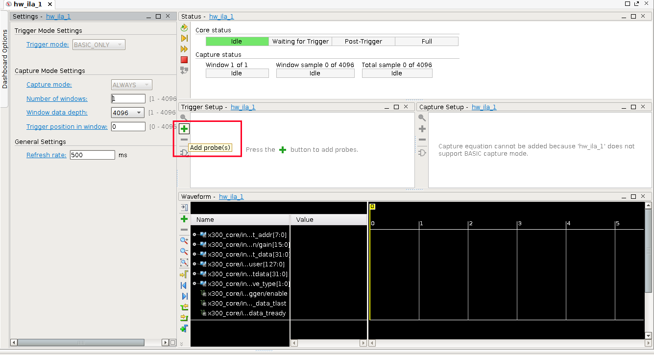
Here we are going to choose two signals as triggers, which are s_axis_data_tvalid and s_axis_data_tready. The names are almost self explanatory: they state when the device has valid data and when it is ready (see [4] for further information). After choosing this signals, now we have to put our device to work. Even, you can click on "run trigger for this ILA core", which will let the device on idle state waiting for the trigger.
Debugging at run time
This is what we came for. The block is to be put in a normal use case where it will run and, simultaneously, we will probe signals from it. For the RFNoC: Signal Generator, we are going to use GNURadio to set up the application. Actually, we are going to use the siggen example that is shipped within gr-ettus. We open to {fpga-repository}{path_to_gr-ettus}/examples/rfnoc/rfnoc_siggen.grc, where a simple setup is ready to show the siggen working.
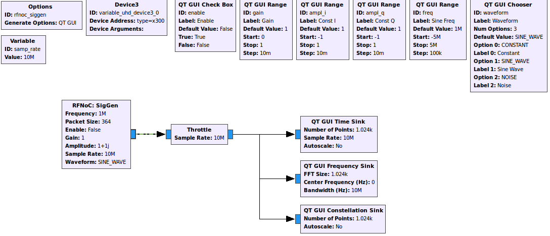
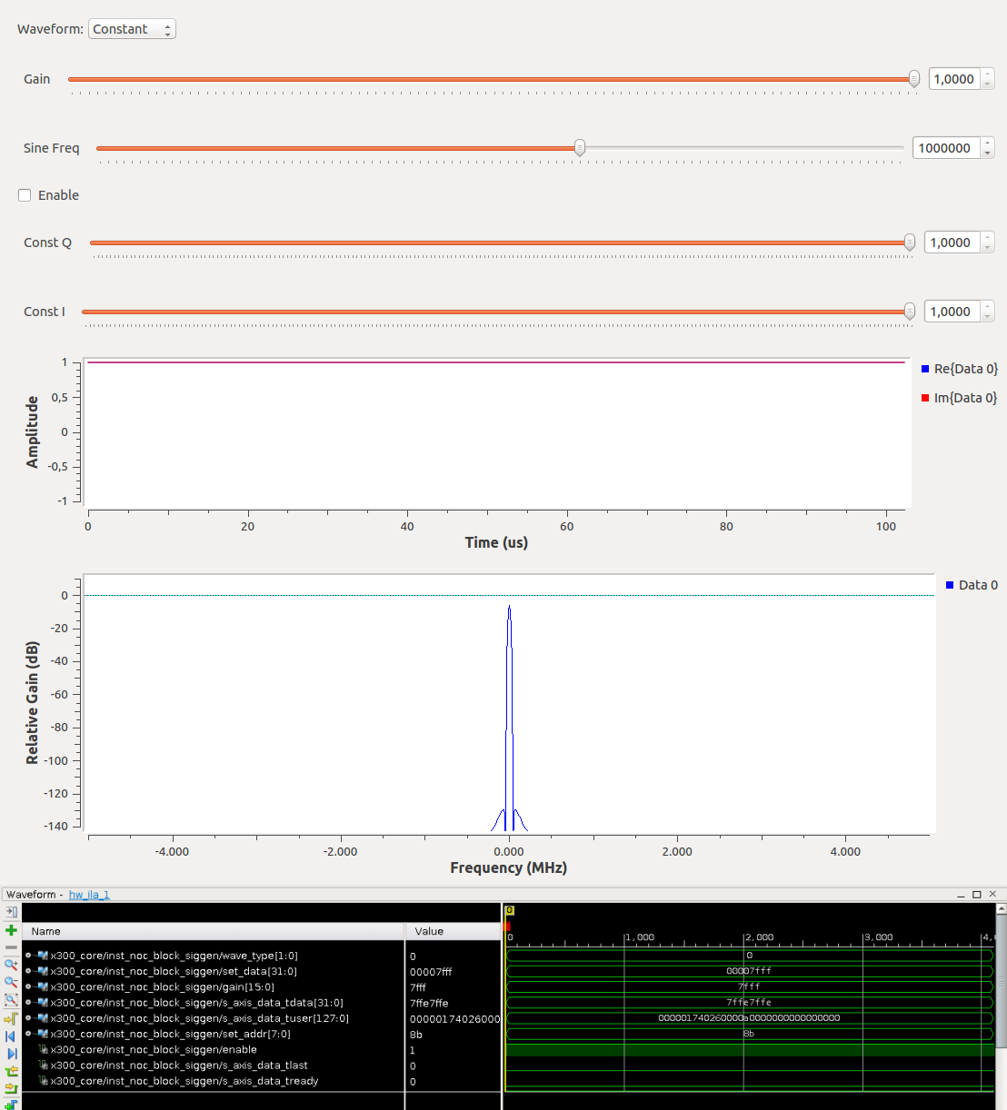
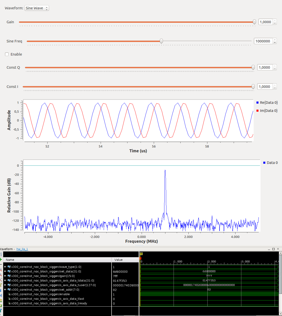
You can see that there is a number of options which can be modified. As we choose to check how signal such as "Wave type" and "gain", we are going to focus on this for now. They can be modified on runtime, but every time that they are set to a different value the trigger has to be run again on the Vivado chipscope. Following are some of the expected results:
Signal type: Constant || Gain: 1: In this case the signal "wave type" is set to 0, as it being the first option available in the block. The Gain is set to 7FFF, which is the maximum hexadecimal value that the register is able to receive in this case and which means the maximum absolute gain.
Signal type: Sinusoid || Gain: 1: Now the wave type is set to 1, being the next option available. The gain is unchanged to show how it holds the same value in the readback register.
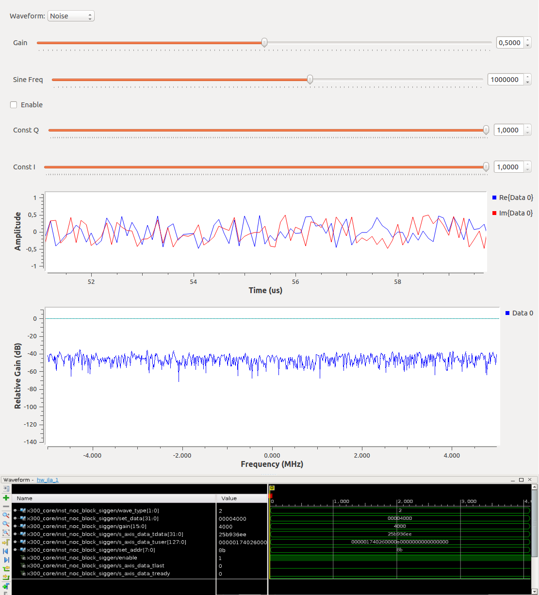
Signal type: Noise || Gain: 0.5: Wave type and gain are both changed, showing results somewhat expected: wave type is set to 2, being sequentially the next option available, and the gain is set to half of the maximum value, which is shown to be true also in its hexadecimal representation read from the readback register.
If you have come successfully until this point, then you can play around with the signals and checking the result in the debugging panel or, even better, apply this technique to debug your own RFNoC design!
External references
[1] Vivado Tutorial: Programming and debugging
[2] Vivado Synthesis
[4] Xilinx - AXI reference guide
[6] LogiCORE IP ChipScope Pro Integrated Logic Analyzer