About Sampling Rates and Master Clock Rates for the USRP X440
Contents
- 1 Application Note Number and Authors
- 2 Overview
- 3 USRP X440 Configuration Considerations
- 4 Use cases
- 5 Appendix
- 6 Footnotes
Application Note Number and Authors
AN-055 by Marian Koop and Martin Anderseck
Overview
This application note guides users through the selection process of Master Clock Rates (MCR) for the USRP X440. It will highlight possible implications and side effects as well as design specific differences to other USRPs (like the X410).
USRP X440 Configuration Considerations
The USRP X440 is a balun-coupled transceiver without built-in RF signal conditioning. Compared to other RF architectures this enables the USRP X440 to access the full RF bandwidth available to the ADC/DAC, but also requires additional frequency planning. To achieve this, the USRP X440 utilizes its ADC/DAC in direct sampling mode and is susceptible to various effects that may distort the signal of interest. These can be separated into distortions from both signal processing and from the ADC/DAC design.
Relationship between RF-ADC/DAC Converter Rate, USRP Master Clock Rate (MCR), Data IQ rate
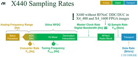
Except for the 200 MHz variant, the default USRP X440 FPGA images do not contain a configurable DDC[1]/DUC[2] block. This means that the IQ sample rate (FIQ) is the same as the Master Clock Rate (MCR) that goes into the RFNoC Radio block. However, unlike most other USRPs the USRP X440 supports a highly variable MCR. The RF Data Converter sampling rate (FS) is chosen by UHD based on the MCR and the available resampling factors of 2, 4, or 8, and defaults to the highest achievable values with these factors. This can be overridden if the desired MCR can be achieved with multiple converter rates (see device argument converter_rate). The inverse calculation - divide the converter rate by 8, 4 or 2 - has to be done to derive the master clock rate if a specific converter rate shall be used. Figure 1 depicts the simplified signal path block diagram for the USRP X440.
Aliases and Nyquist Zones
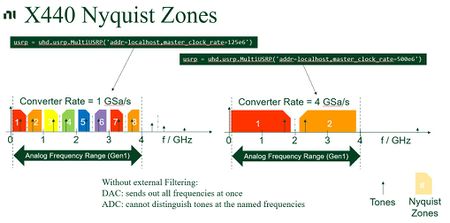
By itself the USRP X440 can sample input signals at frequencies above the Nyquist frequency[3], which is half of the ADC converter sampling rate (FS). However, this method introduces aliasing effects, which cause unwanted signals to appear as mirror images around multiples of the Nyquist frequency (FS/2) in the output spectrum. The first Nyquist zone (N1) is the frequency range from 0 to FS/2, and the second Nyquist zone (N2) goes from FS/2 to FS. Other Nyquist zones are numbered in ascending order, each spanning FS/2. The digital passband in each Nyquist zone can be calculated as 0.4 * FS (see also [4]). The following figure depicts the Nyquist zones for the minimum and maximum RF-ADC converter rates supported by the USRP X440. Note that the illustrations do not show the effects of external, analog filters on the achievable passband within a Nyquist zone. A typical expectation is, that the unusable frequency range around each Nyquist zone boundary (also often referred to as a guard band) increases with ascending Nyquist zone order and results in decreasing, lopsided achievable passbands.
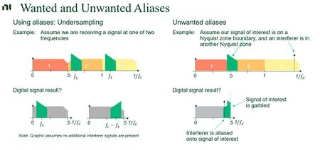
Knowledge of signal aliases can both be exploited and create uncertainties. Applications could utilize intentional under sampling (also referred as "bandpass sampling") to receive signals at greater than FS/2. The same effect may on the other hand lead to garbled or distorted signal detection if the signal of interest spans multiple Nyquist zones or interferer signals are aliased into the observed spectrum. Both effects are depicted in figure 3.
Applications should therefore prefer converter rates that can contain the desired signal spectrum in a single Nyquist zone, or split the signal spectrum among multiple channels and devices. While the USRP X440 does not limit the utilized Nyquist zone, performance degrades in higher orders zones and application should focus on operating in Nyquist zones 1 and 2 (For RX, zone 3 is possible, but zones 4 and higher result into significant performance degradation).
RF-ADC Spurs to consider and how to predict them
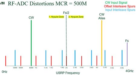
Another kind of distortion originates from the ADC/DAC itself. The USRP X440 uses the Xilinx RFDC, which is a design that combines multiple converters to achieve high RF-ADC rates. An RF-ADC in this design has 8 sub-ADCs that are interleaved together. The resulting offset spurs are minimized by the integrated self-calibration (see also [5]) executed by UHD but may still be detectable in the signal spectrum.
Even with the best calibration the RF-ADC spurs may still be detectable in the captured spectrum. Knowledge of the location of the spurs, in particular the RF-ADC offset spur may be used during frequency planning to select an MCR (and converter rate) that exclude the offset spur frequencies from the capture spectrum. RF-ADC input spurs on the other hand will be more difficult to avoid, but as rule of thumb for modulated input signals carrier frequencies that fall on an RF-ADC offset spur frequency should be avoided (because offset and input spurs would superimpose each other).
How to predict offset spurs
Any residual DC offset not corrected appears as a spur at k*FS/N, where FS is the composite converter rate of the RF-ADC, N is the number of sub-RF-ADCs interleaved together (8 for X4xx devices), and k = 0, 1, 2, … N. For more information on expected spurs levels, refer to OIS at [6].
How to predict input spurs
Any residual difference from gain and time skew correction results in spurious signals at +/-fin + (k/N)*FS, where FS is the converter rate of the RF-ADC, N is the number of sub-RF-ADCs (8 for X4xx devices), and fin is the frequency of the input signal. For more information on expected spurs levels, refer to GTIS at [7].
RF-DAC Distortions
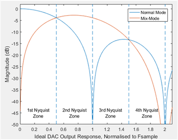
Like the RF-ADC, the RF-DAC is also not an ideal circuitry and suffers from zero-order hold reconstruction. To counter this undesired attenuation in all but the first Nyquist zone, the Xilinx RF-DAC offers a Mix-Mode, which improves the power response in the second Nyquist zone and is utilized by the USRP X440. This, together with an inverse sinc filter to counter residual distortion limits the practical use of the RF-DAC to the first two Nyquist zones. For more information on the RF-DAC mix-mode and inverse sinc filter characteristics, refer to [8].
Note: Due to the direct sampling architecture without filters on the FBX daughterboard, TX ports will output the converter rate (Fc) with a low power (<-50 dBm) as soon as the corresponding ADCs and DACs are enabled, even if the DACs are not actively transmitting. This is a known limitation of the X440 and FBX design. For instance when acquiring a signal on the RX1 port of RF0, the converter rate (Fc) can be measured on the TX/RX0 port of RF0. While operation around the converter rate (Fc) is not recommended anyway, it is possible to suppress the converter rate (Fc) by using a frontend module with a sufficiently high attenuation at the converter rate.
Dual Rate
Unlike previous USRPs, the USRP X440 supports the operation at two different master clock rates simultaneously. All channels on the first daughterboard will run on the first master clock rate / sampling rate and all channels on the second daughterboard will run on the second configured master clock rate / sampling rate. The main motivation for having two different master clock rates is the direct sampling architecture of the USRP X440 without signal conditioning and filtering. While Aliases and Nyquist Zones describes the challenges of that, with dual rate this feature can be used to capture an RF spectrum that exceeds the bandwidth abilities of the single rate operation. Using a second rate, one can close the Nyquist gap of the other and monitor a wider spectrum for further processing. As the clocks of both radios are derived from a common clocking chip, not all combinations are possible. Refer to X440 Supported Dual Rates for possible RF Data Converter sampling rate combinations. The section about the Relationship between RFADC/DAC Converter Rate, USRP Master Clock Rate (MCR) and Data IQ rate explains how to derive valid master clock rates from the RF Data converter sampling rates.
Note: When using different MCRs for both daughterboards, the device will skip the multi-tile synchronization. That means that the phase relationship between channels may not be preserved over retunes and reboots for channels of the same daughterboard and no defined phase relationship will be preserved between channels of different daughterboards.
Use cases
Scan Spectrum within single Nyquist zone
Spectrum Capture between 1.7 and 1.9 GHz.
- Min Bandwidth: 200 MHz
- Minimum IQ Rate: 250 MSps
Option 1: MCR = 250 MHz, RF-ADC converter rate = 2 GHz
This is not the best option because our spectrum of interest is very close to a Nyquist zone boundary.
Option 2: MCR = 300 MHz, RF-ADC converter rate = 2.4 GHz
This option is better, the spectrum of interest is well within a Nyquist zone. Within the bandwidth of interest falls one of the ADC offset spurs. If the input signal is relatively strong, the impact from this small spur is negligible. If on the other hand the input signal strength is on the low end (for the X440), then maybe a different MCR should be considered.
Option 3: MCR = 320 MHz, RF-ADC converter rate = 2.56 GHz
This option avoids a potential impact of an ADC offset spur in the observed spectrum. The only drawback to option 2 is the slightly higher data rate during host post-processing.
Spectrum Capture between 500 MHz and 1.5 GHz.
The USRP X440 ships with multiple FPGA image flavors. These either support 400 MHz or 1600 MHz RF bandwidth per channel. To address this use case, users have the option of using a bit file with 1600 MHz RF bandwidth to capture a contiguous spectrum, or use a 400 MHz bit file and create a stitched spectrum during host side post-processing.
Using 1600 MHz image
- Min Bandwidth: 1000 MHz
- Minimum IQ Rate: 1250 MSps
Option 1: MCR = 1280 MHz, RF-ADC converter rate = 2.56 GHz
Bad option, because desired spectrum spans multiple Nyquist zones.
Option 2: MCR = 1600 MHz, RF-ADC converter rate = 3.2 GHz
This is not the best option because our spectrum of interest is very close to a Nyquist zone boundary.
Option 3: MCR = 1689.6 MHz, RF-ADC converter rate = 3.3792 GHz
This option would work. If the input signal strength is low, using an even higher MCR would reduce the number of potential ADC offset spurs. This needs to be traded off against a higher data rate during host post-processing.
Using 400 MHz image
Due to the smaller bandwidth addressing the use case will require the use of multiple channels. The captured spectra than needs to be stitched (combined) together.
- Max Bandwidth: 400 MHz
Option 1: MCR 400 MHz, RF-ADC converter rate = 3.2 GHz, 3 channels
This is not the best option because our spectrum of interest boundary is very close to a Nyquist zone boundary.
Option 2: MCR 450 MHz, RF-ADC converter rate = 3.6 GHz, 3 channels
This option would work. Since the spectrum of interest is larger than the per channel bandwidth the captured spectrum may contain potential ADC offset spurs. For the spectrum of interest the 3 channels would nicely use tune frequencies (680, 1000, 1320 MHz) that do not match ADC offset spur frequencies.
Option 3: MCR 512 MHz, RF-ADC converter rate = 4.096 GHz, 3 channels
This option would work as well. Like in option 2, the spectrum of interest may contain one potential ADC offset spur (compared to 2 in option 2). The drawback to option 2 is of course again the higher data rate during host post-processing that may be offset by only having to stitch less spectra (2 vs 3) together.
Scan Spectrum with dual master clock rate
Spectrum capture between 1.0 and 2.4 GHz (L-band)
- Combination of two RF-ADC converter rates: 4096 MHz and 2560 MHz
- Derived master clock rates: 1024 MHz (resampling factor 4) and 1280 MHz (resampling factor 2). The resampling factors are chosen to produce master clock rates which allow capturing a sufficient bandwidth to not have any gaps.
- Center frequencies: 1.23 GHz and 2.0 GHz respectively
- 1600 MHz FPGA image required due to the bandwidth requirements
In the picture you can see a light-green band between 1.0 GHz and 2.4 GHz which can be covered using two different rates: Radio0 operates at MCR=1024 MHz in its first Nyquist zone and radio1 operates at 1280 MHz in its second Nyquist zone. The coverage is shown as light-blue boxes in both frequency charts. Starting with UHD 4.6, the X440_L_band_capture.py example demonstrates this use case and by default uses center frequencies of 0.9 GHz and 2 GHz respectively. These were choosen to conveniently display the two individual spectra next to each other in a continuous spectra view without any overlap. Practical applications on the other hand need to take into account that the well usable bandwidth of each channel is only about 0.8 * MCR. For the chosen MCRs this means that the first radio has a usable bandwidth of 819.2 MHz and the second one of 1024 MHz. Taking into account that a typical RF passband in the first Nyquist zone has a passband of up to 0.4 * FS and the need for some overlap of the two spectra, the center frequency of radio0 should be set to 1.230 GHz (usable bandwidth spans from ~820 MHz to ~1640 MHz). Radio1 will be used in its second Nyquist zone, so the center frequency should be 2.0 GHz (usable bandwidth from ~1.5 GHz to ~2.5 GHz).
Appendix
X440 Supported Master Clock Rates (MCR)
Note: The selected FPGA bitfile may further limit the maximum supported master clock rate.
| MCR (MHz) | RFDC Converter Rate (GHz) |
|---|---|
| 125.0 | 1.0 |
| 128.0 | 1.024 |
| 133.12 | 1.06496 |
| 150.0 | 1.2 |
| 153.6 | 1.2288 |
| 160.0 | 1.28 |
| 163.84 | 1.31072 |
| 184.32 | 1.47456 |
| 199.68 | 1.59744 |
| 200.0 | 1.6 |
| 204.8 | 1.6384 |
| 240.0 | 1.92 |
| 245.76 | 1.96608 |
| 250.0 | 2.0, 1.0 |
| 256.0 | 2.048, 1.024 |
| 266.24 | 2.12992, 1.06496 |
| 300.0 | 2.4, 1.2 |
| 307.2 | 2.4576, 1.2288 |
| 320.0 | 2.56, 1.28 |
| 327.68 | 2.62144, 1.31072 |
| 360.0 | 2.88, 1.44 |
| 368.64 | 1.47456, 2.94912 |
| 375.0 | 3.0, 1.5 |
| 384.0 | 1.536, 3.072 |
| 399.36 | 3.19488, 1.59744 |
| 400.0 | 3.2, 1.6 |
| 409.6 | 3.2768, 1.6384 |
| 450.0 | 1.8, 3.6 |
| 460.8 | 1.8432, 3.6864 |
| 480.0 | 3.84, 1.92 |
| 491.52 | 3.93216, 1.96608 |
| 500.0 | 4.0, 2.0, 1.0 |
| 512.0 | 1.024, 2.048, 4.096 |
| 532.48 | 1.06496, 2.12992 |
| 552.96 | 2.21184, 1.10592 |
| 599.04 | 1.19808, 2.39616 |
| 600.0 | 1.2, 2.4 |
| 614.4 | 1.2288, 2.4576 |
| 625.0 | 1.25, 2.5 |
| 640.0 | 2.56, 1.28 |
| 655.36 | 1.31072, 2.62144 |
| 665.6 | 1.3312, 2.6624 |
| 720.0 | 1.44, 2.88 |
| 737.28 | 1.47456, 2.94912 |
| 750.0 | 1.5, 3.0 |
| 768.0 | 1.536, 3.072 |
| 798.72 | 3.19488, 1.59744 |
| 800.0 | 1.6, 3.2 |
| 819.2 | 3.2768, 1.6384 |
| 840.0 | 1.68, 3.36 |
| 860.16 | 3.44064, 1.72032 |
| 875.0 | 3.5, 1.75 |
| 896.0 | 3.584, 1.792 |
| 900.0 | 1.8, 3.6 |
| 921.6 | 1.8432, 3.6864 |
| 931.84 | 1.86368, 3.72736 |
| 960.0 | 3.84, 1.92 |
| 983.04 | 1.96608, 3.93216 |
| 998.4 | 3.9936, 1.9968 |
| 1000.0 | 4.0, 2.0 |
| 1024.0 | 4.096, 2.048 |
| 1050.0 | 2.1 |
| 1064.96 | 2.12992 |
| 1075.2 | 2.1504 |
| 1080.0 | 2.16 |
| 1105.92 | 2.21184 |
| 1120.0 | 2.24 |
| 1125.0 | 2.25 |
| 1146.88 | 2.29376 |
| 1152.0 | 2.304 |
| 1198.08 | 2.39616 |
| 1200.0 | 2.4 |
| 1228.8 | 2.4576 |
| 1280.0 | 2.56 |
| 1290.24 | 2.58048 |
| 1310.72 | 2.62144 |
| 1331.2 | 2.6624 |
| 1350.0 | 2.7 |
| 1382.4 | 2.7648 |
| 1397.76 | 2.79552 |
| 1400.0 | 2.8 |
| 1433.6 | 2.8672 |
| 1440.0 | 2.88 |
| 1474.56 | 2.94912 |
| 1500.0 | 3.0 |
| 1536.0 | 3.072 |
| 1600.0 | 3.2 |
| 1625.0 | 3.25 |
| 1638.4 | 3.2768 |
| 1650.0 | 3.3 |
| 1658.88 | 3.31776 |
| 1664.0 | 3.328 |
| 1680.0 | 3.36 |
| 1689.6 | 3.3792 |
| 1720.32 | 3.44064 |
| 1730.56 | 3.46112 |
| 1750.0 | 3.5 |
| 1760.0 | 3.52 |
| 1792.0 | 3.584 |
| 1797.12 | 3.59424 |
| 1800.0 | 3.6 |
| 1802.24 | 3.60448 |
| 1843.2 | 3.6864 |
| 1863.68 | 3.72736 |
| 1875.0 | 3.75 |
| 1920.0 | 3.84 |
| 1950.0 | 3.9 |
| 1966.08 | 3.93216 |
| 1996.8 | 3.9936 |
| 2000.0 | 4.0 |
| 2027.52 | 4.05504 |
| 2048.0 | 4.096 |
X440 Supported Master Clock Rate combinations (Dual Rate)
Important: For the best RF performance it is required to configure the master clock rate that is connected to the higher RF-ADC/DAC converter rate on the first radio and the MCR connected to the lower converter rate second. Not all master clock rate combinations listed in this table will comply to this requirement by themselves. Specifying the converter_rate argument or swapping the master clock rates will help resolving issues. The selected FPGA bitfile may further limit the maximum supported master clock rate.
| MCR0 (MHz) | MCR1 (MHz) |
| 125.0 | 250.0, 375.0, 500.0, 750.0, 875.0, 1000.0, 1125.0, 1625.0, 1750.0, 1875.0, 2000.0 |
| 128.0 | 384.0, 512.0, 768.0, 1152.0 |
| 133.12 | 266.24, 399.36, 532.48, 665.6, 798.72, 931.84, 1064.96, 1198.08, 1331.2, 1730.56, 1863.68, 1996.8 |
| 150.0 | 300.0, 450.0, 600.0, 750.0, 900.0, 1050.0, 1350.0, 1500.0, 1650.0, 1800.0, 1950.0 |
| 153.6 | 307.2, 614.4, 1228.8 |
| 160.0 | 320.0, 640.0, 800.0, 1120.0, 1280.0, 1600.0, 1760.0 |
| 163.84 | 327.68, 655.36, 1146.88, 1310.72, 1474.56, 1802.24 |
| 184.32 | 368.64, 552.96, 737.28, 1105.92, 1290.24, 1474.56, 1658.88, 1843.2, 2027.52 |
| 199.68 | 399.36, 599.04, 798.72, 998.4, 1198.08, 1397.76, 1797.12, 1996.8 |
| 200.0 | 400.0, 800.0, 1200.0, 1400.0, 1600.0 |
| 204.8 | 409.6, 819.2, 1433.6, 1638.4 |
| 240.0 | 360.0, 480.0, 600.0, 720.0, 840.0, 960.0, 1440.0, 1680.0, 1800.0, 1920.0 |
| 245.76 | 491.52, 860.16, 983.04, 1720.32, 1966.08 |
| 250.0 | 125.0, 375.0, 500.0, 750.0, 875.0, 1000.0, 1500.0, 1625.0, 1750.0, 1875.0, 2000.0 |
| 256.0 | 640.0, 896.0, 1024.0, 1280.0, 1664.0, 1792.0, 2048.0 |
| 266.24 | 133.12, 399.36, 532.48, 665.6, 798.72, 931.84, 1064.96, 1331.2, 1730.56, 1863.68, 1996.8 |
| 300.0 | 150.0, 450.0, 600.0, 750.0, 900.0, 1050.0, 1500.0, 1650.0, 1800.0, 1950.0 |
| 307.2 | 153.6, 614.4, 1228.8 |
| 320.0 | 160.0, 640.0, 800.0, 1120.0, 1280.0, 1600.0, 1760.0 |
| 327.68 | 163.84, 655.36, 1146.88, 1310.72, 1802.24 |
| 360.0 | 240.0, 600.0, 720.0, 1080.0, 1800.0 |
| 368.64 | 184.32, 552.96, 737.28, 1105.92, 1290.24, 1474.56, 1658.88, 1843.2, 2027.52 |
| 375.0 | 125.0, 250.0, 750.0, 1125.0, 1500.0, 1875.0 |
| 384.0 | 128.0, 768.0, 1152.0, 1536.0 |
| 399.36 | 133.12, 199.68, 266.24, 599.04, 665.6, 798.72, 998.4, 1198.08, 1331.2, 1397.76, 1797.12, 1996.8 |
| 400.0 | 200.0, 800.0, 1200.0, 1400.0, 1600.0 |
| 409.6 | 204.8, 819.2, 1433.6, 1638.4 |
| 450.0 | 150.0, 300.0, 600.0, 750.0, 900.0, 1350.0, 1500.0, 1800.0 |
| 460.8 | 768.0, 921.6, 1075.2, 1382.4, 1536.0 |
| 480.0 | 240.0, 720.0, 840.0, 960.0, 1440.0, 1680.0, 1920.0 |
| 491.52 | 245.76, 860.16, 983.04, 1720.32, 1966.08 |
| 500.0 | 125.0, 250.0, 750.0, 875.0, 1000.0, 1500.0, 1750.0, 2000.0 |
| 512.0 | 128.0, 768.0, 1536.0 |
| 532.48 | 133.12, 266.24, 798.72, 931.84, 1064.96, 1331.2, 1863.68 |
| 552.96 | 184.32, 368.64, 737.28, 1105.92, 1290.24, 1474.56, 1658.88, 1843.2 |
| 599.04 | 199.68, 399.36, 798.72, 998.4, 1198.08, 1397.76, 1797.12, 1996.8 |
| 600.0 | 150.0, 240.0, 300.0, 360.0, 450.0, 720.0, 900.0, 1000.0, 1050.0, 1500.0, 1800.0, 2000.0 |
| 614.4 | 153.6, 307.2, 1228.8 |
| 640.0 | 160.0, 256.0, 320.0, 800.0, 1120.0, 1280.0, 1600.0 |
| 655.36 | 163.84, 327.68, 1146.88, 1310.72 |
| 665.6 | 133.12, 266.24, 399.36, 798.72, 1331.2, 1996.8 |
| 720.0 | 240.0, 360.0, 480.0, 600.0, 960.0, 1440.0, 1680.0, 1800.0, 1920.0 |
| 737.28 | 184.32, 368.64, 552.96, 1105.92, 1290.24, 1474.56, 1843.2 |
| 750.0 | 125.0, 150.0, 250.0, 300.0, 375.0, 450.0, 500.0, 900.0, 1000.0, 1125.0, 1500.0, 1750.0, 1875.0, 2000.0 |
| 768.0 | 128.0, 384.0, 460.8, 512.0, 921.6, 1152.0, 1536.0 |
| 798.72 | 133.12, 199.68, 266.24, 399.36, 532.48, 599.04, 665.6, 998.4, 1064.96, 1198.08, 1331.2, 1397.76, 1863.68, 1996.8 |
| 800.0 | 160.0, 200.0, 320.0, 400.0, 640.0, 1200.0, 1400.0, 1600.0 |
| 819.2 | 204.8, 409.6, 1433.6, 1638.4 |
| 840.0 | 240.0, 480.0, 1680.0 |
| 860.16 | 245.76, 491.52, 1720.32 |
| 875.0 | 125.0, 250.0, 500.0, 1750.0 |
| 896.0 | 256.0, 1792.0 |
| 900.0 | 150.0, 300.0, 450.0, 600.0, 750.0, 1500.0, 1800.0 |
| 921.6 | 460.8, 768.0, 1536.0 |
| 931.84 | 133.12, 266.24, 532.48, 1863.68 |
| 960.0 | 240.0, 480.0, 720.0, 1440.0, 1920.0 |
| 983.04 | 245.76, 491.52, 1966.08 |
| 998.4 | 199.68, 399.36, 599.04, 798.72, 1198.08, 1996.8 |
| 1000.0 | 125.0, 250.0, 500.0, 600.0, 750.0, 1500.0, 2000.0 |
| 1024.0 | 256.0, 1280.0, 2048.0 |
| 1050.0 | 150.0, 300.0, 600.0 |
| 1064.96 | 133.12, 266.24, 532.48, 798.72, 1331.2 |
| 1075.2 | 460.8 |
| 1080.0 | 360.0 |
| 1105.92 | 184.32, 368.64, 552.96, 737.28, 1474.56, 1658.88, 1843.2 |
| 1120.0 | 160.0, 320.0, 640.0 |
| 1125.0 | 125.0, 375.0, 750.0, 1500.0, 1875.0 |
| 1146.88 | 163.84, 327.68, 655.36 |
| 1152.0 | 128.0, 384.0, 768.0, 1536.0 |
| 1198.08 | 133.12, 199.68, 399.36, 599.04, 798.72, 998.4, 1797.12, 1996.8 |
| 1200.0 | 200.0, 400.0, 800.0, 1600.0 |
| 1228.8 | 153.6, 307.2, 614.4 |
| 1280.0 | 160.0, 256.0, 320.0, 640.0, 1024.0, 1600.0 |
| 1290.24 | 184.32, 368.64, 552.96, 737.28 |
| 1310.72 | 163.84, 327.68, 655.36 |
| 1331.2 | 133.12, 266.24, 399.36, 532.48, 665.6, 798.72, 1064.96, 1996.8 |
| 1350.0 | 150.0, 450.0 |
| 1382.4 | 460.8 |
| 1397.76 | 199.68, 399.36, 599.04, 798.72 |
| 1400.0 | 200.0, 400.0, 800.0 |
| 1433.6 | 204.8, 409.6, 819.2 |
| 1440.0 | 240.0, 480.0, 720.0, 960.0, 1920.0 |
| 1474.56 | 163.84, 184.32, 368.64, 552.96, 737.28, 1105.92 |
| 1500.0 | 150.0, 250.0, 300.0, 375.0, 450.0, 500.0, 600.0, 750.0, 900.0, 1000.0, 1125.0, 2000.0 |
| 1536.0 | 384.0, 460.8, 512.0, 768.0, 921.6, 1152.0 |
| 1600.0 | 160.0, 200.0, 320.0, 400.0, 640.0, 800.0, 1200.0, 1280.0 |
| 1625.0 | 125.0, 250.0 |
| 1638.4 | 204.8, 409.6, 819.2 |
| 1650.0 | 150.0, 300.0 |
| 1658.88 | 184.32, 368.64, 552.96, 1105.92 |
| 1664.0 | 256.0 |
| 1680.0 | 240.0, 480.0, 720.0, 840.0 |
| 1720.32 | 245.76, 491.52, 860.16 |
| 1730.56 | 133.12, 266.24 |
| 1750.0 | 125.0, 250.0, 500.0, 750.0, 875.0 |
| 1760.0 | 160.0, 320.0 |
| 1792.0 | 256.0, 896.0 |
| 1797.12 | 199.68, 399.36, 599.04, 1198.08 |
| 1800.0 | 150.0, 240.0, 300.0, 360.0, 450.0, 600.0, 720.0, 900.0 |
| 1802.24 | 163.84, 327.68 |
| 1843.2 | 184.32, 368.64, 552.96, 737.28, 1105.92 |
| 1863.68 | 133.12, 266.24, 532.48, 798.72, 931.84 |
| 1875.0 | 125.0, 250.0, 375.0, 750.0, 1125.0 |
| 1920.0 | 240.0, 480.0, 720.0, 960.0, 1440.0 |
| 1950.0 | 150.0, 300.0 |
| 1966.08 | 245.76, 491.52, 983.04 |
| 1996.8 | 133.12, 199.68, 266.24, 399.36, 599.04, 665.6, 798.72, 998.4, 1198.08, 1331.2 |
| 2000.0 | 125.0, 250.0, 500.0, 600.0, 750.0, 1000.0, 1500.0 |
| 2027.52 | 184.32, 368.64 |
| 2048.0 | 256.0, 1024.0 |
References and Related Documentation
- Advantages of Direct RF Sampling Architectures
- Zynq UltraScale+ RFSoC RF Data Converter v2.6 Gen 1/2/3/DFE LogiCORE IP Product Guide (PG269)
- GRcon 23 - Lo and behold, no LO!
- Zynq UltraScale+ RFSoC Data Sheet: DC and AC Switching Characteristics (DS926)
Footnotes
- ↑ Digital Down Conversion
- ↑ Digital Up Conversion
- ↑ Nyquist frequency
- ↑ Xilinx RF-ADC Decimation Filters (Gen-1)
- ↑ Key CAL Features and Guidance Summary
- ↑ RF-ADC Performance Characteristics
- ↑ RF-ADC Performance Characteristics
- ↑ RF-DAC Nyquist Zone Operation
- ↑ Xilinx: Ideal DAC Output Response, Normalised to Fsample

