E310/E312
Contents
- 1 Device Overview
- 2 Key Features
- 3 Daughterboard Specifications
- 4 RF Specifications
- 5 Hardware Specifications
- 6 Physical Specifications
- 7 Environmental Specifications
- 8 Schematics
- 9 Key Component Datasheets
- 10 Mechanical Information
- 11 FPGA
- 12 Interfaces and Connectivity
- 13 E312 Battery
- 14 Certifications
- 15 Certificate of Volatility
- 16 SD Card Images
- 17 Security Notes
- 18 Additional Resources
- 19 Downloads
Device Overview
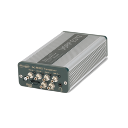
The USRP E310 offers a portable stand-alone SDR platform designed for field deployment. The flexible 2x2 MIMO AD9361 transceiver from Analog Devices provides up to 56 MHz of instantaneous bandwidth and spans frequencies from 70 MHz – 6 GHz to cover multiple bands of interest.
Key Features
E310
|
E312
|
Daughterboard Specifications
E310 MIMO XCVR board
The USRP E310 MIMO XCVR daughterboard features an integrated MIMO capable RF frontend.
Tuning
The RF frontend has individually tunable receive and transmit chains. Both transmit and receive can be used in a MIMO configuration. For the MIMO case, both receive frontends share the RX LO, and both transmit frontends share the TX LO. Each LO is tunable between 50 MHz and 6 GHz.
Gains
All frontends have individual analog gain controls. The receive frontends have 76 dB of available gain; and the transmit frontends have 89.5 dB of available gain. Gain settings are application specific, but it is recommended that users consider using at least half of the available gain to get reasonable dynamic range.
LO lock status
The frontends provide a lo-locked sensor that can be queried through the UHD API.
// assumes 'usrp' is a valid uhd::usrp::multi_usrp::sptr instance
// get status for rx frontend
usrp->get_rx_sensor("lo-locked");
// get status for tx frontend
usrp->get_tx_sensor("lo-locked");
Filter and Antenna Switches
The transmit and receive filter banks uses switches to select between the available filters. These paths are also dependent on the antenna switch settings. Incorrectly setting the switches generally results in attenuated input / output power. Receive filters are band pass (series high & low pass filters), transmit filters are low pass.
Source code related to controlling the filter band and antenna switches resides in e300_impl.c. Specifically, refer to methods e300_impl::_update_bandsel, e300_impl::_update_atrs, e300_impl::_update_gpio, and e300_impl::_update_enables. Generally, these methods set the switches depending on the state of transmit and receive streams.
The following sections provide switch setting tables for antenna and filter selection for frontends A & B receive and transmit paths. For futher details refer to the schematics.
Side A Filter and Antenna Switches
Note: X = don't care, T = If full duplex, set bits according to transmit table, otherwise don't care. Filter range A – B will be selected if A <= freq < B.
Receive
| RX Port | RX Filter (MHz) | VCTXRX2_V1,V2 | VCRX2_V1,V2 | RX2_BANDSEL[2:0] | RX2B_BANDSEL[1:0] | RX2C_BANDSEL[1:0] |
|---|---|---|---|---|---|---|
| TRX-A | < 450 | 01 | 10 | 101 | XX | 01 |
| TRX-A | 450 – 700 | 01 | 10 | 011 | XX | 11 |
| TRX-A | 700 – 1200 | 01 | 10 | 001 | XX | 10 |
| TRX-A | 1200 – 1800 | 01 | 10 | 000 | 01 | XX |
| TRX-A | 1800 – 2350 | 01 | 10 | 010 | 11 | XX |
| TRX-A | 2350 – 2600 | 01 | 10 | 100 | 10 | XX |
| TRX-A | 2600 – 6000 | 01 | 01 | XXX | XX | XX |
| RX2-A | 70 – 450 | TT | 01 | 101 | XX | 01 |
| RX2-A | 450 – 700 | TT | 01 | 011 | XX | 11 |
| RX2-A | 700 – 1200 | TT | 01 | 001 | XX | 10 |
| RX2-A | 1200 – 1800 | TT | 01 | 000 | 01 | XX |
| RX2-A | 1800 – 2350 | TT | 01 | 010 | 11 | XX |
| RX2-A | 2350 – 2600 | TT | 01 | 100 | 10 | XX |
| RX2-A | >= 2600 | TT | 10 | XXX | XX | XX |
Transmit
| TX Port | TX Filter (MHz) | VCTXRX2_V1,V2 | TX_ENABLE2A,2B | TX_BANDSEL[2:0] |
|---|---|---|---|---|
| TRX-A | < 117.7 | 10 | 01 | 111 |
| TRX-A | 117.7 – 178.2 | 10 | 01 | 110 |
| TRX-A | 178.2 – 284.3 | 10 | 01 | 101 |
| TRX-A | 284.3 – 453.7 | 10 | 01 | 100 |
| TRX-A | 453.7 – 723.8 | 10 | 01 | 011 |
| TRX-A | 723.8 – 1154.9 | 10 | 01 | 010 |
| TRX-A | 1154.9 – 1842.6 | 10 | 01 | 001 |
| TRX-A | 1842.6 – 2940.0 | 10 | 01 | 000 |
| TRX-A | >= 2940.0 | 11 | 10 | XXX |
Note: Although the transmit filters are low pass, this table describes UHD's tuning range for selecting each filter path. The table also includes the required transmit enable state.
Side B Filter and Antenna Switches
Note: X = don't care, T = If full duplex, set bits according to transmit table, otherwise don't care. Filter range A – B will be selected if A <= freq < B.
Receive
| RX Port | RX Filter (MHz) | VCTXRX1_V1,V2 | VCRX1_V1,V2 | RX1_BANDSEL[2:0] | RX1B_BANDSEL[1:0] | RX1C_BANDSEL[1:0] |
|---|---|---|---|---|---|---|
| TRX-B | < 450 | 10 | 01 | 100 | XX | 10 |
| TRX-B | 450 – 700 | 10 | 01 | 010 | XX | 11 |
| TRX-B | 700 – 1200 | 10 | 01 | 000 | XX | 01 |
| TRX-B | 1200 – 1800 | 10 | 01 | 001 | 10 | XX |
| TRX-B | 1800 – 2350 | 10 | 01 | 011 | 11 | XX |
| TRX-B | 2350 – 2600 | 10 | 01 | 101 | 01 | XX |
| TRX-B | 2600 – 6000 | 10 | 10 | XXX | XX | XX |
| RX2-B | 70 – 450 | TT | 10 | 100 | XX | 10 |
| RX2-B | 450 – 700 | TT | 10 | 010 | XX | 11 |
| RX2-B | 700 – 1200 | TT | 10 | 000 | XX | 01 |
| RX2-B | 1200 – 1800 | TT | 10 | 001 | 10 | XX |
| RX2-B | 1800 – 2350 | TT | 10 | 011 | 11 | XX |
| RX2-B | 2350 – 2600 | TT | 10 | 101 | 01 | XX |
| RX2-B | >= 2600 | TT | 01 | XXX | XX | XX |
Transmit
| TX Port | TX Filter (MHz) | VCTXRX1_V1,V2 | TX_ENABLE1A,1B | TX1_BANDSEL[2:0] |
|---|---|---|---|---|
| TRX-B | < 117.7 | 00 | 01 | 111 |
| TRX-B | 117.7 – 178.2 | 00 | 01 | 110 |
| TRX-B | 178.2 – 284.3 | 00 | 01 | 101 |
| TRX-B | 284.3 – 453.7 | 00 | 01 | 100 |
| TRX-B | 453.7 – 723.8 | 00 | 01 | 011 |
| TRX-B | 723.8 – 1154.9 | 00 | 01 | 010 |
| TRX-B | 1154.9 – 1842.6 | 00 | 01 | 001 |
| TRX-B | 1842.6 – 2940.0 | 00 | 01 | 000 |
| TRX-B | >= 2940.0 | 11 | 10 | XXX |
Note: Although the transmit filters are low pass, the following table describes UHD's tuning range for selecting each filter path. The table also includes the required transmit enable states.
RF Specifications
RF Performance
- SSB/LO Suppression -35/50 dBc
- Phase Noise 3.5 GHz 1.0 deg RMS
- Phase Noise 6 GHz 1.5 deg RMS
- Power Output >10dBm
- IIP3 (@ typ NF) -20dBm
- Typical Noise Figure <8dB
Input/Output Impedance
- All RF Ports are matched to 50 Ohm with -10dB or better return loss generally. Detailed test is pending.
Hardware Specifications
- Ettus Research recommends to always use the latest stable version of UHD
E310
- Current Hardware Revision: 1
- Minimum version of UHD required: 3.8.0
- Required version on the host computer must match what is running on the E310
E312
- Current Hardware Revision: 1
- Minimum version of UHD required: 3.8.5
- Required version on the host computer must match what is running on the E312
Physical Specifications
Dimensions
- 133 x 68 x 26.4 mm
Environmental Specifications
Operating Temperature Range
- E310 0-40 °C
- E312 0-40 °C
Operating Humidity Range
- 10% to 90% non-condensing
Schematics
E310
Key Component Datasheets
| Part Number | Description | Schematic ID (Page) |
|---|---|---|
| Motherboard | ||
| TXS02612RTWR | SDIO PORT EXPANDER | U23 (2) |
| XC7Z020-1CLG484CES9919 | FPGA | U11 (2,3,4,8,11,13) |
| Xilinx Zynq Product Page | FPGA | - |
| USB3340-EZK-TR | ULPI Transceiver | U33 (5) |
| AK4571VQP | Audio CODEC | U30 (6) |
| FT230XQ-R | UART Interface | U32 (6) |
| 88E1512 | Gigabit Ethernet Transceiver | U13 (7) |
| 24LC024/SN | EEPROM | U5 (9) |
| DS1339,SM | Real-Time Clock | U6 (9) |
| ADT7408 | Temperature Sensor | U8 (9) |
| MPU-9150 | Motion Processing Unit | U3 (9) |
| InvenSense MPU-9150 Product Page | Motion Processing Unit | U3 (9) |
| BMP180 | Digital pressure sensor | U4 (9) |
| BQ24192 | Adapter Charger | U1 (10) |
| TPS54478 | Step-Down Switcher | U20 (10) |
| MAX6510HAUT-T | Temperature Switches | U35 (10) |
| ATTINY88-MU | Microcontroller | U18 (10) |
| TPS61253YFF | Step-Up Converter | U19 (10) |
| AMY-6M | GPS Module | U12 (6) |
| Daughterboard | ||
| Part Number | Description | Schematic ID (Page) |
| AD9361 Product Page | 2 x 2 RF Agile Transceiver | U8 (3) |
| 24AA256 | EEPROM | U15 (2) |
| TC-1-43A+ | RF Transformer | T6 (3); T5 (3); T4 (3) |
| TC1-1-13M+ | RF Transformer | T7 (3); T10 (3); T1 (3) |
| TPS62140 | Step-Down Converter | U19 (4) |
| ADP1753ACPZ-R7 | Linear Regulator | U17 (4); U18 (4) |
| SGA-4563Z | MMIC AMPLIFIER | U12 (5); U4 (5) |
| SKY13418-485LF | Antenna Switch | U13 (5); U3 (5); U16 (5); U2 (5); U10 (6); U5 (6) |
| SKY13373-460LF | SP3T Switch | U11 (6); U9 (6); U6 (6); U7 (6); SW4 (7); SW1 (7) |
| MGA-81563 | Amplifier | U14 (5); U1 (5) |
| LFCN-5850+ | Low Pass Filter | FL32 (5); FL1 (5) |
| LFCN-2750+ | Low Pass Filter | FL37 (5); FL4 (5) |
| LFCN-2250+ | Low Pass Filter | FL23 (6); FL20 (6) |
| LFCN-1700+ | Low Pass Filter | FL40 (5); FL2 (5) |
| LFCN-1575+ | Low Pass Filter | FL25 (6); FL17 (6) |
| LFCN-1000+ | Low Pass Filter | FL33 (5); FL9 (5); FL27 (6); FL15 (6) |
| LFCN-575+ | Low Pass Filter | FL36 (5); FL5 (5) |
| LFCN-530+ | Low Pass Filter | FL29 (6); FL13 (6) |
| LFCN-400+ | Low Pass Filter | FL38 (5); FL3 (5); FL30 (6); FL11 (6) |
| LFCN-225 | Low Pass Filter | FL39 (5); FL6 (5) |
| LFCN-160+ | Low Pass Filter | FL34 (5); FL8 (5) |
| LFCN-80+ | Low Pass Filter | FL35 (5); FL7 (5) |
| HFCN-1600+ | High Pass Filter | FL22 (6); FL19 (6) |
| HFCN-1100+ | High Pass Filter | FL24 (6); FL16 (6) |
| HFCN-650+ | High Pass Filter | FL26 (6); FL14 (6) |
| HFCN-440+ | High Pass Filter | FL28 (6); FL12 (6) |
| BFCN-2435+ | Bandpass Filter | FL21 (6); FL18 (6) |
| FDG6301N | Dual N-Channel, Digital FET | Q8 (7); Q5 (7) |
| HSMS-8202 | Mixer Diodes | CR1 (7); CR2 (7); CR3 (7); CR4 (7) |
| LP5900TL | Linear Regulator | U25 (8) |
| ADP150AUJZ-3.0 | Linear Regulator | U22 (8) |
| AD5662RBJ | 16-Bit nanoDAC | U21 (8) |
| SN74AUP1T57 | Voltage Translator | U27 (8); U28 (8); U29 (8) |
Request a detailed whitepaper covering features and components from [email protected]
Mechanical Information
Weight
- Partial Enclosure 225 g
- Full Enclosure 375 g
Drawings
E310
- File:E310 Dimensional Sketches.pdf
- File:cu e310 motherboard cca.pdf
- File:cu E310 daughtercard cca.pdf
- File:cu usrp-e310.pdf
E312
FPGA
- Utilization statistics are subject to change between UHD releases. This information is current as of UHD 3.9.4 and was taken directly from Xilinx Vivado 2014.4.
E310/E312
1. Slice Logic
--------------

+----------------------------+-------+-----------+-------+
|          Site Type         |  Used | Available | Util% |
+----------------------------+-------+-----------+-------+
| Slice LUTs                 | 36203 |     53200 | 68.05 |
|   LUT as Logic             | 28108 |     53200 | 52.83 |
|   LUT as Memory            |  8095 |     17400 | 46.52 |
|     LUT as Distributed RAM |   870 |           |       |
|     LUT as Shift Register  |  7225 |           |       |
| Slice Registers            | 36562 |    106400 | 34.36 |
|   Register as Flip Flop    | 36562 |    106400 | 34.36 |
|   Register as Latch        |     0 |    106400 |  0.00 |
| F7 Muxes                   |   376 |     26600 |  1.41 |
| F8 Muxes                   |   125 |     13300 |  0.93 |
+----------------------------+-------+-----------+-------+

3. Memory
---------

+-------------------+------+-----------+-------+
|     Site Type     | Used | Available | Util% |
+-------------------+------+-----------+-------+
| Block RAM Tile    |   97 |       140 | 69.28 |
|   RAMB36/FIFO*    |   90 |       140 | 64.28 |
|     RAMB36E1 only |   90 |           |       |
|   RAMB18          |   14 |       280 |  5.00 |
|     RAMB18E1 only |   14 |           |       |
+-------------------+------+-----------+-------+
* Note: Each Block RAM Tile only has one FIFO logic available and therefore can accommodate only one FIFO36E1 or one FIFO18E1. However, if a FIFO18E1 occupies a Block RAM Tile, that tile can still accommodate a RAMB18E1


4. DSP
------

+----------------+------+-----------+-------+
|    Site Type   | Used | Available | Util% |
+----------------+------+-----------+-------+
| DSPs           |  120 |       220 | 54.54 |
|   DSP48E1 only |  120 |           |       |
+----------------+------+-----------+-------+
Interfaces and Connectivity
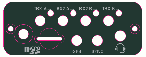
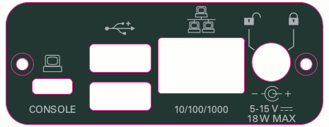
- 10/100/1000 BASE-T Ethernet
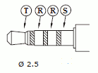
- Stereo audio out, mono mic in
- Integrated GPS receiver
- Host USB support
- 9-axis IMU
Front Panel
Rear Panel
|
|
GPIO
|
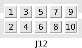
Pin Mapping
|
|
- Please see the E3x0/X3x0 GPIO API for information on configuring and using the GPIO bus.
Audio
E312 Battery
The USRP E312 is equipped with an integrated 3.7V, 3200mAh lithiumion battery cell. After unboxing the USRP E312 , plug in the power adapter to an AC power source and fully charge the battery. This process with take approximately 2 hours. Do not leave the USRP E312 unit plugged in for more than 24 hours.
The status LED in the power button indicates the power and charge status of the battery:
Off: Indicates device is off and not charging.
- Slow Blinking Green: Indicates device is off and charging.
- Fast Blinking Green: Indicates device is on and charging.
- Solid Green: Indicates device is on and not charging (Battery is finished charging).
- Solid Orange: Indicates device is on and discharging.
- Fast Blinking Orange: Indicates device is on, discharging, and charge is below 10% charge.
- Fast Blinking Red: Indicates an error code:
- Low Voltage Error
- Regulator Low Voltage Error
- FPGA Power Error
- DRAM Power Error
- 1.8V Power Rail Error
- 3.3V Power Rail Error
- Daughterboard / TX Power Error
- Charger Error
- Charger Temperature Error
- Battery Low Error
- Fuel Gauge Temperature Error
- Global (Enclosure) Temperature Error
The battery life of the USRP E312 in idle mode is approximately 5 1/2 hours. The battery will enable the USRP E312 to operate for approximately 2 hours 20 minutes, when transmitting and receiving on both channels (2x2 MIMO), with maximum gain settings, at 5 GHz center frequency, and 1 MS/s sample rate. When the power button status LED is in the “Fast Blinking Orange” mode, plug the USRP E312 into an AC power source as soon as possible to recharge the battery.
If the power button status LED indicates a “Low Voltage Error” (codes 1, 2, 3, 4, 5, 6, 7) or a “Battery Low Error” (code 10), plug the USRP E312 into an AC power source as soon as possible to recharge the battery.
When the power button status LED indicates at “Temperature Error” or “Charger Error” (codes 8, 9, 11, or 12), power off the USRP E312 unit and allow it to cool down to room temperature. Then, plug in the USRP E312 to and AC power source and fully charge the battery.
If error codes persist after cooling down and/or recharging the USRP E312, please contact [email protected].
You can purchase a replacement battery for the E312 at https://www.ettus.com/product/details/E312-battery.
An Application Note covering the replacement of the E312 battery can be found at USRP E312 Battery Replacement Instructions.
Certifications
RoHS
As of December 1st, 2010 all Ettus Research products are RoHS compliant unless otherwise noted. More information can be found at http://ettus.com/legal/rohs-information
Certificate of Volatility
E310
E312
SD Card Images
The E31x SD card images can be obtained two ways:
- Using uhd_images_downloader. See these instructions: https://files.ettus.com/manual/page_usrp_e3xx.html#update_sdcard
- Direct download from https://files.ettus.com/binaries/cache/e3xx/
Note: Obsolete images, such as the alpha, beta, and Release 4 images, are located here: https://files.ettus.com/e3xx_images/. These release are no longer supported and provided here for archival purposes only.
If choosing to directly download the SD card image, please note that they are sorted by UHD version with the format meta-ettus-vUHD_VERSION. For example, the UHD 4.5 release is meta-ettus-v4.5.0.0. Each release contains SD card images and the SDK (OE cross-compiler build environment) for the USRP E31x. There is a manifest file that shows which packages, and which versions, are included in the OE build within each folder.
We highly recommend customers use UHD 4.5 or later. It is fine if you are already successfully using an older version, but at some point it is recommended that you upgrade to a current version so that you benefit from the latest bug fixes, new features, stability improvements, and other enhancements.
The UHD 4.5+ release images include UHD 4.5 (or later), GNU Radio 3.8, Python 3, and the corresponding FPGA image file.
Note: An 8 GB SD card is required for the Release 4 image.
The SD card image contains both the FPGA image and the OS for the E31x. The FPGA image is located in the file system of the E31x in the /usr/local/share/uhd/images directory.
The E31x image comes in two speed grade varieties, sg1 and sg3. The majority of USRP E31x devices use the sg3 image, but older devices may use sg1. The version that you will need depends on the product number of your E31x, which is printed on the bottom of the device.
| E310 (15633X-01L) | X= A, B, C, D | e3xx_e310_sg1 |
| X= E or later | e3xx_e310_sg3 | |
| E312 (140605X-01L) | X = All | e3xx_e310_sg3 |
For the E310, the product number will be 156333X-01L, where X is a letter from A to Z. For devices where X is A, B, C, D, the image starting with e3xx_e310_sg1 should be used. For devices where X is E or later, the images under the e3xx_e310_sg3 folder should be used. You must use the appropriate image for your specific device. The incorrect image will not work, and will only boot as far as the U-Boot boot loader before stopping.
For the E312, the product number will be 140605X-01L, where X is a letter from A to Z. The image starting with e3xx_e310_sg3 folder should be used for all E312 devices.
You can burn the image to an SD card using the "dd" tool. Instructions on how to use this tool are located at the links below:
The SD image files have an *.zip extension. You can uncompress these files with any zip compatible tool, such as 7-Zip. Please see the links below for further information.
7-Zip
Security Notes
The OpenEmbedded project reported a security vulnerability for OE-Core (http://lists.openembedded.org/pipermail/openembedded-architecture/2017-June/000638.html). If you are an USRP E-Series user that is building binary ipkgs which you then distribute to your customers, you may be affected by this issue. No other workflows are impacted.
The vulnerability is documented as CVE-2017-9731 (https://cve.mitre.org/cgi-bin/cvename.cgi?name=2017-9731). The specific issue is that information in the SRC_URI for software repositories used by OE recipes is "leaked" by binary ipkgs. For example, if you are using the E-Series OE-generated SDK to build binary ipkgs, and the URI you use for your source code repository contains sensitive information (e.g., https://github.com/company-name/secret-project-name, or local-server.internal.com?USER=admin&PASSWORD=password), then that information will be leaked in the Source: field of the ipkg.
The OpenEmbedded team has merged a fix for this into OE-Core master, and backported the change to previous versions of OpenEmbedded. Generally, including sensitive information in the SRC_URIs is not a good idea, and we highly recommend users avoid doing this in their build process. Some recommendations provided on the OpenEmbedded discussion list:
- Use non-confidential path names (i.e., don’t include confidential customer or project names in build paths).
- Change or manage the host name of your build system so that it is non-confidential, like
build-1instead ofsecret-product.my-company.internal.com. - Use a "build user" who does not have network credentials to access sensitive machines during the build process.
If you have any questions about this, or need help determining if this issue affects you, please let us know by contacting [email protected].


