USRP-2974
Contents
- 1 Device Overview
- 2 Key Features of the USRP-2974
- 3 Controller - Onboard computer
- 4 RF Specifications
- 5 Hardware Specifications
- 6 Physical Specifications
- 7 Power
- 8 Environmental Specifications
- 9 System Diagram and Schematics
- 10 Key Component Datasheets
- 11 FPGA and Baseband
- 12 Interfaces and Connectivity
- 13 Certifications
- 14 Downloads
- 15 Choosing an Interface
- 16 GPS Disciplined, Oven-Controlled Oscillator (GPSDO)
- 17 Option: Using the GPIO Expansion Kit
- 18 Option: Antenna Kit for GPSDO
- 19 Option: Cables for MIMO Expansion
- 20 FAQ
Device Overview
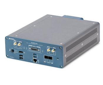
The NI USRP-2974 is a high-performance, USRP software defined radio (SDR) stand-alone device for designing and deploying next generation wireless communications systems. The hardware architecture combines two extended-bandwidth daughterboard slots covering 10 MHz – 6 GHz with up to 160 MHz of baseband bandwidth, multiple high-speed interface options (PCIe, dual 10 GigE), an onboard Intel Core i7 processor, and a large user-programmable Kintex-7 FPGA in a convenient desktop or rack-mountable half-wide 2U form factor.
The USRP-2974 is the equivalent to a USRP X310 with two UBX-160 boards, a GPSDO and an onboard Intel i7 computer. The USRP-2974 comes with NI Linux RTOS pre-installed, but in order to use it with open-source tool-chain, a user will need to install Linux (preferably Fedora or Ubuntu) and then the USRP Hardware driver (UHD). After these have been installed, any other open-source tools can be installed, such as GNU Radio.
Key Features of the USRP-2974
|
Controller - Onboard computer
| System on module (SoM) | Congatec COM Express conga-TS170 |
| CPU | Intel Core i7 6822EQ (2 GHz Quad Core) |
| Memory | SO-DIMM DDR4 16 GB |
| SFP+1 | 10G ETH connection to the SoM |
| Cabled PCIe | PCIe Gen 2 x4 |
| MicroUSB2 | USB-to-UART to the SoM |
| RJ45 | 1G ETH host connection |
1 Can be bypassed to the FPGA.
2 Device port for external host.
RF Specifications
| Transmitter | |
|---|---|
| Number of channels | 2 |
| Frequency range | 10MHz to 6GHz |
| Frequency step | <1kHz |
| Maximum output power | 5mW to 100mW (7dBm to 20dBm) |
| Gain range1 | 0dB to 31.5dB |
| Gain step | 0.5dB |
| Maximum instantaneous real-time bandwidth | 160MHz |
| Receiver | |
|---|---|
| Number of channels | 2 |
| Frequency range | 10MHz to 6GHz |
| Frequency step | <1kHz |
| Gain range2 | 0dB to 37.5dB |
| Gain step | 0.5dB |
| Maximum input power | 10dBm |
| Noise Figure | 5dB to 7dB |
| Maximum instantaneous real-time bandwidth3 | 160MHz |
1 The output power resulting from the gain setting varies over the frequency band and among devices.
2The received signal amplitude resulting from the gain setting varies over the frequency band and among devices.
3The USRP-2974 receiver path has 84 MHz of bandwidth for center frequencies from 10 MHz to 500 MHz
NOTE: As mentioned earlier, the USRP-2974 incorporates 2 UBX-160 daughterboards. Therefore, for more information on RF performance, please see the UBX hardware resource page
Hardware Specifications
USRP Hardware Driver (UHD) version
- Minimum version of UHD required: 3.15.0
Clocking and Sampling Rates
There are two master clock rates (MCR) supported on the USRP-2974 like on the X310: 200.0 MHz and 184.32 MHz.
The sampling rate must be an integer decimation rate of the MCR. Ideally, this decimation factor should be an even number. An odd decimation factor will result in additional unwanted attenuation (roll-off from the CIC filter in the DUC and DDC blocks in the FPGA). The valid decimation rates are between 1 and 1024.
For the MCR of 200.0 MHz, the achievable sampling rates using an even decimation factor are 200.0, 100.0, 50.0, 33.33, 25.0, 20.0, 16.67, 14.286 Msps, ... 195.31 Ksps.
For the MCR of 184.32 MHz, the achievable sampling rates using an even decimation factor are 184.32, 92.16, 46.08, 30.72, 23.04, 18.432, 15.36, 13.166 Msps, ... 180.0 Ksps.
If the desired sampling rate is not directly supported by the hardware, then it will be necessary to re-sample in software. This can be done in C++ using libraries such as Liquid DSP [1], or can be done in GNU Radio, in which there are three blocks that perform sampling rate conversion.
Physical Specifications
Dimensions
(L × W × H) 29.08 cm × 21.84 cm × 7.98 cm (11.45 in. × 8.60 in. × 3.14 in. )
Weight
3.34 kg (7.35 lb)
Power
| Voltage range | 14.25 V to 15.75 V DC |
| Current | 10 A, maximum |
| Power | 150 W, maximum |
Environmental Specifications
NOTE: Indoor use only
Operating Temperature Range
- 0 °C to 50 °C
Maximum altitude
- 2,000 m (800 mbar) (at 25 °C ambient temperature)
Operating Humidity Range
- 10% to 90% non-condensing
Pollution Degree
- 2
System Diagram and Schematics
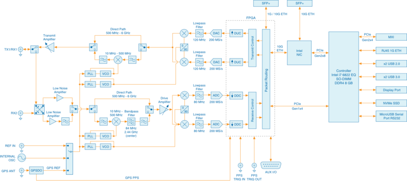
System Block Diagram
Schematics
Because the USRP-2974 is a combination of an Intel i7 SOM and an X310 USRP, a user can reference the X310 Schematics.
Key Component Datasheets
| Part Number | Description | Schematic ID (Page) |
|---|---|---|
| conga-TS170 | System on Module (SoM) | |
| XC7K410T | FPGA | U23 (3,5,8,9,10,18) |
| AD9146 | Dual Channel, 16-Bit, 1230 MSPS DAC | U12, U36 (7) |
| ADS62P48 | Dual Channel, 14-Bit 210 MSPS ADC | U11, U35 (6) |
| FIN1002 | High Speed Differential Receiver | U3, U5, U31, U32 (4) |
| 24LC256T | EEPROM | U530 (11) |
| LMK04816BISQ/NOPB_1/3 | Jitter Cleaner With Dual Loop PLLs | U531 (11) |
| SY89547LMGTR | Multiplexer | U506 (12) |
| SN74AUP1T17 | Single Schmitt-Trigger Buffer Gate | U6, U519 (12) |
| TPS54620RGYT | Synchronous Step Down SWIFT™ Converter | U515 (21); U516 (26) |
| LT1764EQ-3.3 | Voltage Regulator | U27 (21); U516 (26) |
| TPS7A47 | Voltage Regulator | U28, U532 (21) |
| LTC3603EUF_TRPBF | Monolithic Synchronous Step-Down Regulator | U517 (23); U500 (25); U514, U513 (27) |
| TPS77625 | Low-Dropout Voltage Regulators | U30 (23) |
| TPS79318_SM | Low-Dropout Voltage Regulators | U510 (27) |
| OSC-96MHZ-724821-01 | Voltage Controlled Crystal Oscillator | U25 (11) |
FPGA and Baseband
| FPGA | Kintex-7 XC7K410T |
| DRAM | 1 GB |
| Baseband analog-to-digital converter
(ADC) resolution |
14 bit |
| Baseband digital-to-analog converter
(DAC) resolution |
16 bit |
| ADC spurious-free dynamic range (sFDR) | 88 dB |
| DAC sFDR | 80 dB |
| Maximum I/Q sample rate | 200 MS/s |
| SFP+1 | High speed serial link to one of the FPGA
GTX transceivers |
1Can be bypassed to the SoM if using the 10 GbE as protocol.
FPGA User Modifications
The Verilog code for the FPGA in the NI USRP-2974 is open-source, and users are free to modify and customize it for their needs. However, certain modifications may result in either bricking the device, or even in physical damage to the unit. Specifically, changing the I/O interface of the FPGA in any way (do not remove any of the I/O for the PCIe interface, such as x300_pcie_int and LvFpga_Chinch_Interface), or modifying the pin and timing constraint files, could result in physical damage to other components on the motherboard, external to the FPGA, and doing this will void the warranty. Also, even if the PCIe interface is not being used, you cannot remove or reassign these pins in the constraint file. The constraint files should not be modified. Please note that modifications to the FPGA are made at the risk of the user, and may not be covered by the warranty of the device.
Interfaces and Connectivity
Follow the links below for additional information on configuring each interface for the USRP-2974.
- Dual 10 Gigabit Ethernet - 200 MS/s Full Duplex @ 16-bit
- PCIe Express (Desktop) - 200 MS/s Full Duplex @ 16-bit
- 1 Gigabit Ethernet - 25 MS/s Full Duplex @ 16-bit
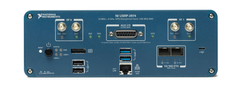
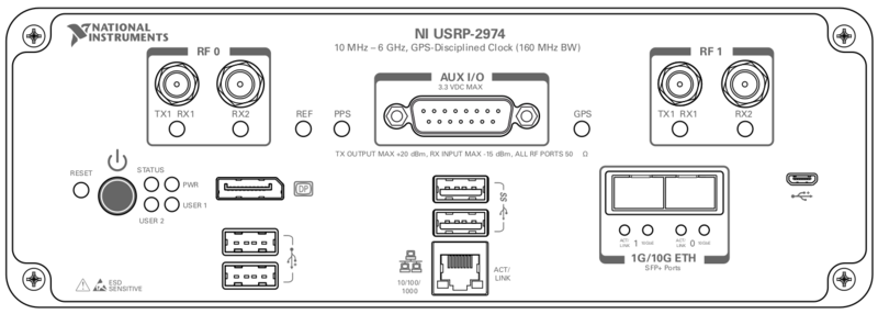
Front Panel
| Connector | Use | |
|---|---|---|
| RF 0 | TX1 RX1 |
Input and output terminal for the RF signal. TX1 RX1 is an SMA (f) connector with an impedance of 50 Ω and is a single-ended input or output channel. |
| RX2 | Input terminal for the RF signal. RX2 is an SMA (f) connector with an impedance of 50 Ω and is a single-ended input channel. | |
| AUX I/O | General-purpose I/O (GPIO) port. AUX I/O is controlled by the FPGA. | |
| RF 1 | TX1 RX1 |
Input and output terminal for the RF signal. TX1 RX1 is an SMA (f) connector with an impedance of 50 Ω and is a single-ended input or output channel. |
| RX2 | Input terminal for the RF signal. RX2 is an SMA (f) connector with an impedance of 50 Ω and is a single-ended input channel. | |
| DP | DisplayPort connector to connect one monitor for your controller. | |
| USB2.0 | USB ports that support common USB peripheral devices such as flash drives, hard drives, keyboards, and mice. | |
| USB3.0 | USB ports that support common USB peripheral devices such as flash drives, hard drives, keyboards, and mice. | |
| 1G ETH | RJ45 port used for 1G ETH connectivity to other ethernet devices. | |
| μUSB | USB port used for UART connectivity to the controller. | |
| 1G/10G ETH 0 | SFP+ port used for 10G ETH connectivity to other ethernet devices. Connects to the embedded Linux computer for communication with LabVIEW RT. | |
| 1G/10G ETH 1 | SFP+ port used for 1G/10G ETH connectivity to other ethernet devices. Connects to the FPGA. Not currently supported in LabVIEW Communications System Design Suite. | |
| LED | Description | Color | State | Indication | |
|---|---|---|---|---|---|
| RF 0 | TX1 RX1 |
Indicates thetransmit status of the device | OFF | — | The device is not active. |
| Red | Solid | The device is transmitting data. | |||
| Green | Solid | The device is receiving data. | |||
| RX2 | Indicates the receive status of the device. | OFF | — | The device is not receiving data. | |
| Green | Solid | The device is receiving data. | |||
| REF | Indicates the status of the reference signal. | OFF | — | There is no reference signal, or the device is not locked to the reference signal. | |
| Green | Blinking | The device is not locked to the reference signal. | |||
| Solid | The device is locked to the reference signal. | ||||
| PPS | Indicates the pulse per second (PPS). | OFF | — | There is no PPS timing reference signal, or the device is not locked to the reference signal. | |
| Green | Blinking | The device is locked to the PPS timing reference signal. | |||
| GPS | Indicates whether the GPSDO is locked. | OFF | — | There is no GPSDO or the GPSDO is not locked. | |
| Green | Solid | The GPSDO is locked. | |||
| RF 1 | TX1 RX1 |
Indicates thetransmit status of the device | OFF | — | The device is not active. |
| Red | Solid | The device is transmitting data. | |||
| Green | Solid | The device is receiving data. | |||
| RX2 | Indicates the receive status of the device. | OFF | — | The device is not receiving data. | |
| Green | Solid | The device is receiving data. | |||
| Status | Indicates the status of the device | OFF | — | The device initialized successfully and is ready for use. | |
| Red | Blinking | Hardware error. An internal power supply has failed. Check front-panel I/O connections for shorts. Remove any shorts and cycle power to the USRP-2974. Contact NI if the problem persists. | |||
| PWR | Indicates the power status of the device | OFF | — | The device is powered off. | |
| Green | Solid | The devices is powered on. | |||
| 10/100/1000 | Indicates the speed of the Gigabit Ethernet link. | OFF | — | No link, or 10 Mbps link. | |
| Green | Solid | 100 Mbps link. | |||
| Amber | Solid | 1,000 Mbps link. | |||
| ACT/LINK | Indicates the Gigabit Ethernet link activity or status. | OFF | — | No link has been established. | |
| Green | Solid | A link has been negotiated. | |||
| Blinking | Activity on the link. | ||||
| 1G/10G ETH 0 | ACT/LINK | Indicates the status of the SFP+ port. | OFF | — | The link is down. |
| Green | Solid | The link is up. | |||
| Blinking | The link is active (transmitting and receiving). | ||||
| 10GbE | Indicates the status of the 10G ETH link. | OFF | — | The 10G ETH link is down. | |
| Green | Solid | The 10G ETH link is up. | |||
| 1G/10G ETH 1 10GbE | Indicates the status of the 10G ETH link. | OFF | — | The 10G ETH link is down. | |
| Green | Solid | The 10G ETH link is up. | |||
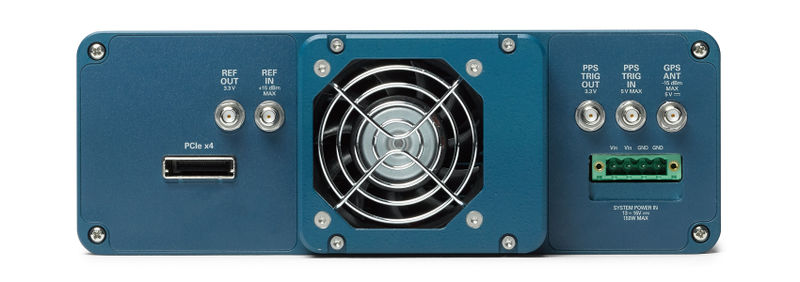
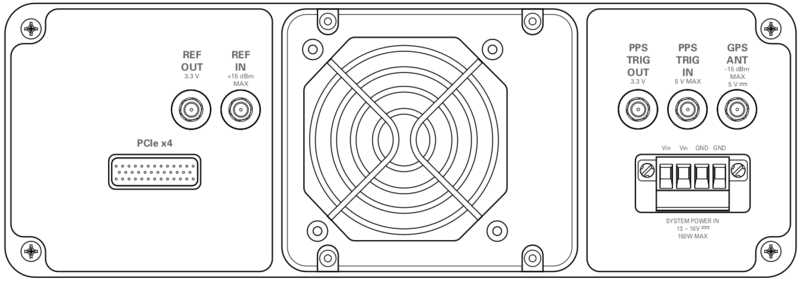
Rear Panel
| Connector | Use |
|---|---|
| REF OUT | Output terminal for an external reference signal for the LO on the device. REF OUT is an SMA (f) connector with an impedance of 50 Ω, and it is a single-ended reference output. The output signal at this connector is 10 MHz at 3.3 V. |
| REF IN | Input terminal for an external reference signal for the LO on the device. REF IN is an SMA (f) connector with an impedance of 50 Ω, and it is a single-ended reference input. REF IN accepts a 10 MHz signal with a minimum input power of 0 dBm (0.632 Vpk-pk) and a maximum input power of 15 dBm (3.56 Vpk-pk) for a square wave or sine wave. |
| PPS TRIG OUT | Output terminal for the PPS timing reference. PPS TRIG OUT is an SMA (f) connector with an impedance of 50 Ω and is a single-ended input. The output signal is 0 V to 3.3 V TTL. You can also use this port as a triggered output (TRIG OUT) that you program with the PPS Trig Out I/O signal. |
| PPS TRIG IN | Input terminal for PPS timing reference. PPS TRIG IN is an SMA (f) connector with an impedance of 50 Ω and is a single-ended input channel. PPS TRIG IN accepts 0 V to 3.3 V TTL and 0 V to 5 V TTL signals. You can also use this port as a triggered input (TRIG IN) that you control using NI-USRP software. |
| GPS ANT | Input terminal for the GPS antenna signal. GPS ANT is an SMA (f) connector with a maximum input power of -15 dBm and an output of DC 5 V to power an active antenna. Notice: Do not terminate the GPS ANT port if you do not use it. |
| PCIe x4 | Port for a PCI Express Generation 2, x4 bus connection through an MXI Express four-lane cable. Can be used to connect an external USRP device or external chassis. |
| SYSTEM POWER IN | Input that accepts a 15 V ± 5%, 10 A external DC power connector. |
Ref Clock - 10 MHz
Using an external 10 MHz reference clock, a square wave will offer the best phase noise performance, but a sinusoid is acceptable. The power level of the reference clock cannot exceed +15 dBm.
PPS - Pulse Per Second
Using a PPS signal for timestamp synchronization requires a square wave signal with the following a 5Vpp amplitude.
To test the PPS input, you can use the following tool from the UHD examples:
-
<args>are device address arguments (optional if only one USRP device is on your machine)
cd <install-path>/lib/uhd/examples ./test_pps_input –args=<args>
Front Panel GPIO
|
The GPIO port is not meant to drive big loads. You should not try to source more than 5mA per pin. The +3.3V is for ESD clamping purposes only and not designed to deliver high currents. |

|
Power on state
The hardware power on state and UHD initial state for the front-panel GPIOs is high-Z. For the X3xx, there are no external pull-ups/pull-downs for the GPIO pins, but the FPGAs do have them and they are configured as follows: X3xx: pull-down.
Pin Mapping
- Pin 1: +3.3V
- Pin 2: Data[0]
- Pin 3: Data[1]
- Pin 4: Data[2]
- Pin 5: Data[3]
- Pin 6: Data[4]
- Pin 7: Data[5]
- Pin 8: Data[6]
- Pin 9: Data[7]
- Pin 10: Data[8]
- Pin 11: Data[9]
- Pin 12: Data[10]
- Pin 13: Data[11]
- Pin 14: 0V
- Pin 15: 0V
Note: Please see the E3x0/X3x0 GPIO API for information on configuring and using the GPIO bus.
Certifications
RoHS
As of December 1st, 2010 all NI/Ettus Research products are RoHS compliant unless otherwise noted. More information can be found at http://ettus.com/legal/rohs-information
China RoHS
Management Methods for Controlling Pollution Caused by Electronic Information Products Regulation
Chinese Customers
National Instruments is in compliance with the Chinese policy on the Restriction of Hazardous Substances (RoHS) used in Electronic Information Products. For more information about the National Instruments China RoHS compliance, visit ni.com/environment/rohs_china.
Downloads
Choosing an Interface
The USRP-2974 provides three interface options – 1 Gigabit Ethernet (1 GigE), 10 Gigabit Ethernet (10 GigE), and PCI-Express (PCIe). The PCIe interface is always available regardless of what FPGA image is loaded. Ettus ships two FPGA image variants, the HG or HGS image which has one 1 GigE interfaces and one 10 GigE interfaces, and the XG image which has two 10 GigE interfaces. Generally, Ettus Research recommends using 10 GigE to achieve the maximum throughput available from the USRP-2974. PCIe is recommended for applications that require the lowest possible latency, which is a desirable characteristic for PHY/MAC research. If your application does not require the full bandwidth of the USRP-2974, the 1 GigE interface serves as a cost-effective fall-back option. Ettus Research provides a complete interface kit for each of these options, which is also shown in the following table.
| Interface Performance Summary | |||
|---|---|---|---|
| Interface | Throughput (MS/s @ 16-bit) | Target | Recommended Kit |
| 1 Gigabit | 25 MS/s | Desktop/Laptop | SFP Adapter + GigE Cable |
| 10 Gigabit | 200 MS/s | Desktop | 10 GigE Interface Kit |
| PCI-Express
(PCIe, 4 lane) |
200 MS/S | Desktop | PCI-Express Desktop Kit |
10 Gigabit Ethernet
In order to utilize the dual 10 Gigabit Ethernet interfaces, ensure the XG image is installed (see FPGA Image Flavors). In addition to burning the prerequisite FPGA image, it may also be necessary to tune the network interface card (NIC) to eliminate drops (Ds) and reduce overflows (Os). This is done by increasing the number of RX descriptors (see Linux specific notes).
The benchmark_rate tool can be used to test this capability. Run the following commands to test the X-series USRP over both 10 Gigabit Ethernet interfaces with the maximum rate of 200 Msps per channel:
   cd <install-path>/lib/uhd/examples
   ./benchmark_rate --args="type=x300,addr=<Primary IP>,second_addr=<secondary IP>" --channels="0,1" --rx_rate 200e6
The second interface is specified by the extra argument second_addr.
Recommended 10 Gigabit Ethernet Cards
- Intel X520-DA2
- Intel X520-DA1
- Intel X710-DA2
- Intel X710-DA4
- Mellanox MCX4121A-ACAT
GPS Disciplined, Oven-Controlled Oscillator (GPSDO)
The USRP-2794 has a high-accuracy GPS-disciplined oscillator (GPSDO). The GPSDO improves the accuracy of the internal frequency reference to 20 ppb, or 0.1 ppb if the GPS is synchronized to the GPS constellation. When synchronized to the GPS constellation, all USRP™ devices will also be synchronized in time within 50 ns.
- Support GPSDO NMEA Strings
- JacksonLabs LC_XO
| Internal TCXO | GPS-Disciplined Clock | |
|---|---|---|
| Frequency Reference | TCXO | OCXO |
| Frequency Accuracy | ± 2.5ppm
± 2,500 Hz @ 1 GHz |
± 20 ppb
± 20 Hz @ 1 GHz |
| Frequency Accuracy | ± 0.01ppb | |
| (GPS-Disciplined) | ~ ± 0.01 Hz @ 1 GHz | |
| GPS Time Sync Accuracy | ±50ns to UTC Time** | |
| 10 MHz Reference Phase Drift with GPS Sync | <±20ns After 1 Hour** |
Sensors
You can query the lock status with the gps_locked sensor, as well as obtain raw NMEA sentences using the gps_gprmc, and gps_gpgga sensors. Location information can be parsed out of the gps_gpgga sensor by using gpsd or another NMEA parser.
Option: Using the GPIO Expansion Kit
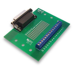
GPIO Expansion Kit Contents
- 1 GPIO Breakout Board
- 1 DB-15, 1-meter cable
- GPIO Quick Reference
Circuit Protection
The GPIO signals exposed with this breakout kit are routed directly to the USRP device's FPGA with limited protection circuitry. However, the user must take precautionary measures to ensure input/output signals meet the specifications shown in this document. Over voltage, excess current draw, and other conditions can damage the USRP device and void the warranty. Special care should be taken when the USRP is powered off.
Mounting the GPIO Breakout Board
The GPIO breakout board can be mounted directly to the DB15 connector of a USRP ™ device, or mounted remotely with the cable provided in this kit. The screws on the DB15 connector of the breakout board must be removed to mount the board directly. For remote mounting, the breakout board is supplied with rubber standoffs to avoid scratching surfaces, and several through-holes for hard mounting with screws or other hardware (not provided).
Using GPIO with UHD, GNU Radio, and other Third-Party Frameworks
When used with UHD, or other third party frameworks that leverage UHD, the GPIO expansion can be controlled with simple API calls. For more information, on the C++ API, and examples of how to use the GPIO in frameworks such as GNU Radio, please see the Application Notes section of the Ettus Research Knowledge Base.
GPIO Specifications (3.3V Bank, LVCMOS)
| Parameter | Typical |
|---|---|
| Configured as Input | |
| Default Voltage Standard | 3.3V LVCMOS |
| Voltage High Threshold | 2.0V |
| Voltage Low Threshold | 0.8V |
| Voltage Input Limits (no damage) | -0.3V/3.45V |
| Configured as Output | |
| Voltage Standard | 3.3V LVCMOS |
| Voltage High Output | 2.8V |
| Voltage Low Output | 0.4V |
| Current Source Capability | 12 mA |
| Output Source Impedance | >33 ohms typical |
Option: Antenna Kit for GPSDO
The GPSDO Mini Kit will improve the accuracy of the USRP reference clock, even if it does not receive signals from the GPS Constellation. However, to achieve the best accuracy possible, and to achieve global timing alignment across multiple USRPs, Ettus Research recommends the GPSDO Mini Antenna Kit.
Option: Cables for MIMO Expansion
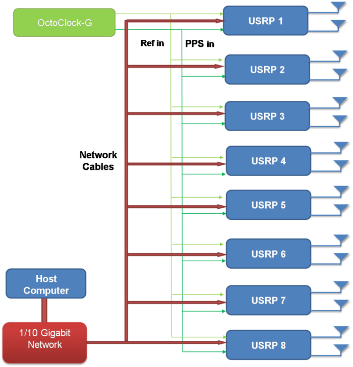
Multiple USRP-2974s can be synchronized for coherent operation by sharing a common 10 MHz and 1 PPS signal. We recommend using a star-distribution topology with an OctoClock or OctoClock-G, as seen in Figure 4. This requires matched length cables to be used for both 10 MHz and 1 PPS.
For more information about MIMO operation, please see the MIMO and Synchronization Application Note.
FAQ
- What is the bandwidth of the USRP-2974
The ADC rate on each analog RX channel is 200 MS/s quadrature, which provides a theoretical analog bandwidth of approximately 80% of the Nyquist bandwidth of +/- 100 MHz (+/- 80 MHz around the center frequency). The resulting maximum theoretical analog bandwidth is 160 MHz.
FPGA Processing Bandwidth: Up to 200 MS/s quadrature.
Host Bandwidth: Up to 200 MS/s quadrature, dependent on selected interface
For more information about achieving the maximum bandwidth with a USRP-2974, please see the "USRP X300/X310 Configuration Guide" or the "USRP System Bandwidth" application note.
- How can I program the USRP-2974
Like all other USRP models, the USRP-2974 is compatible with the USRP Hardware Driver™ (UHD) architecture. The UHD architecture is a common driver that allows users to develop and execute applications on the onboard or host computer. UHD provides a direct C++ API to control and stream to/from the USRP-2974. It also provides compatibility with a variety of third-party software frameworks including GNU Radio, LabVIEW, and MATLAB. You may also customize the FPGA image provided with UHD to integrate your own signal processing. For more information about UHD, and supported software frameworks, please see:
http://files.ettus.com/manual/
- How do I update the FPGA images and firmware with the latest from UHD
You can find more information about updating the FPGA image through PCIe, 1/10 GigE, and JTAG here.
- How can I modify the FPGA of the USRP-2974
The source code (Verilog) for the USRP-2794 is available in the UHD repository. The build process leverages the existing CMAKE build system used to compile the host-side driver. A Linux-based setup will provide the best results.
Which FPGA toolchain required to build the FPGA images will depend upon your version of UHD. For more details please see the UHD Software Resource page.
- How much free space is available in the USRP-2974 FPGA
Please see the #Utilization statistics section of this resources page for more information.
- What frequency range does the USRP-2974 cover
10MHz to 6GHz.
- What components do I need to purchase for a complete USRP-2974 system

